首次揭秘:英特尔制胜未来的半导体前沿技术储备

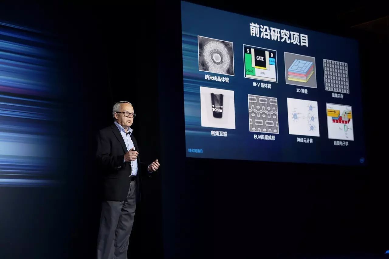
英特尔技术与制造前沿研究项目
本文引用地址:https://www.eepw.com.cn/article/201709/364544.htmIntel’s Components Research team fund sand works with universities and academic research consortia on forward-looking research topics such as Spintronics, and also on the understanding of fundamental science which is the basis of these forward-looking research.
英特尔前沿研究部门资助多家大学院校和学术机构,共同开展多种前沿研究课题,比如自旋电子以及这些前沿研究的基础科学。
英特尔高级院士、技术与制造事业部制程架构与集成总监Mark T. Bohr
解读英特尔前沿研究项目
1Nanowire transistorsare being explored as a future option because the nanowire structure provides improves channel electrostatics that can enable further transistor gate length scaling.
纳米线晶体管被认为是未来技术的一种选择,因为纳米线的结构可提供改进通道静电,从而进一步实现晶体管栅极长度的微缩。
2Silicon has always been the material used in MOSFET channels, but III-V materialssuch as GaAs and InP have improved carrier mobility that can provide higher performance or the ability to operate transistors at lower voltage for lower active power.
硅是MOSFET通道中经常使用的材料,但是III-V 材料(如砷化镓和磷化铟)改进了载流子迁移率,从而提供更高的性能或者能够在更低的电压和更低的有功功耗下运行晶体管。
33D stacking of silicon die can provide system integration opportunities to mix different technologies into a small form factor.
硅晶片的3D堆叠有机会实现系统集成,以便把不同的技术混装到一个很小的地方。
4A variety of dense memory options, including volatile and non-volatile memory, are being explored and developed.
多种不同的高密度内存选择,其中包括易失性和非易失性存储技术,正在探索和开发中。
5Scaling interconnectsis just as important as scaling transistors on advanced process technologies. Novel materials and patterning techniques are being explored to enable dense interconnects.
对于精尖制程工艺来说,微缩互联和微缩晶体管一样重要。新的材料和图案成形技术正在探索中,以支持高密度互联。
6Extreme Ultraviolet (EUV) lithography using a 13.5 nm wavelength is being developed to enable better scaling as today’s 193nm wavelength tools reach their scaling limit.
极紫外(EUV)光刻技术:采用13.5纳米波长。由于当今的193纳米波长工具已达到其微缩极限,该技术正在研发中以实现进一步的微缩。
7Spintronicsis a beyond-CMOS technology that promises very dense and low power circuits that are an option when CMOS can no longer be scaled.
自旋电子是一种超越CMOS的技术,当CMOS无法再进行微缩的时候,这是一种选择,可提供非常密集和低功耗的电路。
8Neuromorphic computingis a different processor design and architecture approach for performing some computing functions with much better power efficiency than today’s computers.
神经元计算是一种不同的处理器设计和架构,能够以比当前计算机高得多的能效执行某些计算功能。


评论