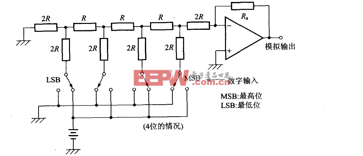
基于FPGA的A/D转换采样控制模块的设计

采用QuartusⅡ软件平台下的VHDL语言编程实现。
library ieee;
use ieee.std_logic_unsigned.all;
use ieee.std_logic_1164.all;
entity ad_hgq is
port( d :in std_logic_vector(7 downto 0);---AD输入;
clk,eoc :in std_logic; ---eoc:转换结束状态信号; oe : buffer std_logic;
addr :out std_logic_vector(2 downto 0); ---oe:输出允许,addr:选通地址;
ale,start:out std_logic; ---ale:允许地址锁存;
q :buffer std_logic_vector(7 downto 0)); ---转换数据输出显示;
end ad_hgq;
architecture behaviour of ad_hgq is
type state is (st0,st1,st2,st3,st4,st5,st6,st7); ---以枚举类型定义各状态子类型;
signal current_state,next_state :state:=st0; signal regl :std_logic_vector(7 downto 0);
signal addrx :std_logic_vector(2 downto 0):=000;
signal lock :std_logic; ---转换后数据输出锁存时钟信号;
signal hex :std_logic_vector(7 downto 0);
begin
process(clk)
begin
if(clk'event and clk='1') then current_state=next_state;
end if; ---在时钟上升沿,转换至下一状态;
end process ; ---由信号current_state将当前状态带出进程,进入下一进程;
process(lock)
begin
if lock='1'and lock'event then regl=d;
end if; --在lock上升沿,将转换好的数据锁存入8位锁存器中;
end process;
process(clk)
begin
if clk'event and clk='1' then
if current_state=st0 then addrx=addrx+1; ---进入下一地址通道;
end if;
end if;
addr=addrx;
end process;
q=regl; ---数据输出;
process(clk)
begin
if( clk'event and clk ='1') then if oe='1' then hex=q; ---将数据送给hex;
end if;
end if;
end process;
end behaviour;
图2显示的是A/D采样控制并将所采的数据转换为BCD码的仿真结果。图中Value为所采的电压结果值。

3 结束语
采用EP1C6T144C8芯片实现对A/D转换器的采样控制,充分利用了FPGA的高速度和高可靠性,从而解决了传统中用单片机控制时速度慢的问题。FPGA具有灵活的编程方式,简单方便的编程环境,易学易用,大大提高工作效率,缩短研制周期。本设计可用于高速应用领域和实时监控方面。


评论