InfineonTLE983x智能汽车继电器驱动解决方案

The TLE983x is a single chip solution that integrates a high performance 8-bit microcontroller derived from the established XC800 family with application specific power drivers, control and communication modules in an automotive qualified new Smart-Power Technology.
The TLE983x family concept offers scalability in terms of Flash memory sizes ranging from 36kB to 64kB with pin-compatible devices.
The TLE983x family was specifically designed to fit to a wide range of LIN-slave applications where a small package form factor and a minimum number of external components is essential.
TLE983x主要特性:
• High performance XC800 core
– compatible to standard 8051 core
– up to 40 MHz clock frequency
– two clocks per machine cycle architecture
– two data pointers
• On-chip memory
– 20, 32, 44 or 60 kByte + 4 kByte Flash for program code and data (4 kByte EEPROM emulation built-in)
– 512 Byte One Time Programmable Memory (OTP)
– 512 Byte 100 Time Programmable Memory (100TP)
– 256 Byte RAM
– 3 kByte XRAM
– BootROM for startup firmware and Flash routines
• Core logic supply at 1.5 V
• On-chip OSC and PLL for clock generation
– Loss of clock detection with fail safe mode for LSS, HSS and LIN
• Watchdog timer (WDT) with programmable window feature for refresh operation and warning prior to overflow
• General-purpose I/O Port (GPIO) with wake-up capability
• Multiplication/division unit (MDU) for arithmetic calculation
• Software libraries to support floating point and MDU calculations
• Five 16-Bit timers - Timer 0, Timer 1, Timer 2, Timer 21 and Timer 3
• Capture/compare unit for PWM signal generation (CCU6) and Hall Sensor measurement with Timer 12 and Timer 13
• Full duplex serial interface (UART) with LIN support
• Synchronous serial channel (SSC)
• On-chip debug support via 2-wire Device Access Port (DAP)
• LIN Bootstrap loader (LIN BSL)
• LIN transceiver compliant to LIN 1.3, LIN 2.0 and LIN 2.1
• 2 x Low Side Switches with clamping capability incl. PWM functionality, e.g. as relay driver
• 1 or 2 x High Side Switches with cyclic sense option and PWM functionality, e.g. for LED or powering of switches
• High Voltage Monitor Input pins for wake-up and with cyclic sense and analog measurement option
• Measurement unit with 10 channels, 8-Bit A/D Converter (ADC2) and data post processing
• 8 channels, 10-Bit A/D Converter (including battery voltage and supply voltage measurement) (ADC1)
• Single power supply from 3.0 V to 27 V
• Low-dropout voltage regulators (LDO)
• Dedicated 5 V voltage regulator for external loads (e.g. hall sensor)
• Programmable window watchdog (WDT1) with independent on-chip clock source
• Optional Operational amplifier for current sensing
• Power saving modes
– MCU slow-down mode
– Stop Mode
– Sleep Mode
– Cyclic wake-up and cyclic sense during Stop Mode and Sleep Mode
• Power-on and undervoltage/brownout reset generator
• Overtemperature protection
• Overcurrent protection with shutdown
• Supported by a full range of development tools including C compilers, macroassembler packages, emulators, evaluation boards, HLL debuggers, programming tools, software packages
• Temperature Range TJ: -40 °C up to 150 °C
• Package PG-VQFN-48
• Green package (RoHS compliant)
TLE983x主要优势:
„„Complete system-on-chip (SoC) for ECU’s that communicate via LIN interface with main ECU
„„High-voltage monitoring inputs for off-board switch control
„„Highly flexible SoC through dedicated configuration registers for e.g. current and voltage settings as well as power saving modes
„„High pin-count VQFN package with 7×7mm footprint enables space saving PCB designs
TLE983x汽车应用:
„„Window Lift
„„Power Seats
„„Sun Roof
„„Fan/Blower Control
„„Key Pad Interface
„„Switch Panel Interface
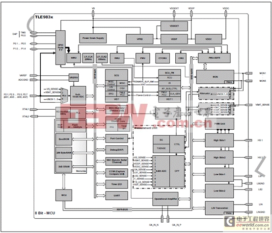
图1.TLE983x方框图
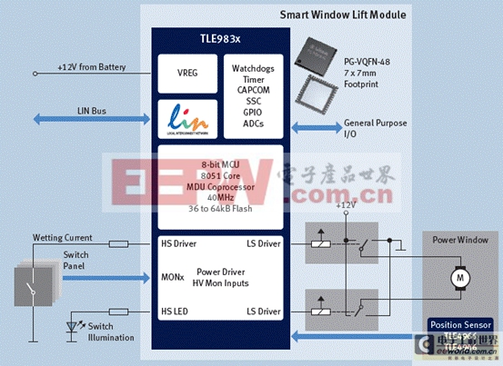
图2.TLE983x智能车窗升降模块框图
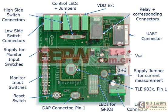
图3.TLE983x评估板外形图

图4.TLE983x评估板电路图(1)
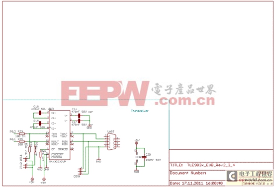
图5.TLE983x评估板电路图(2)
TLE983x评估板材料清单:
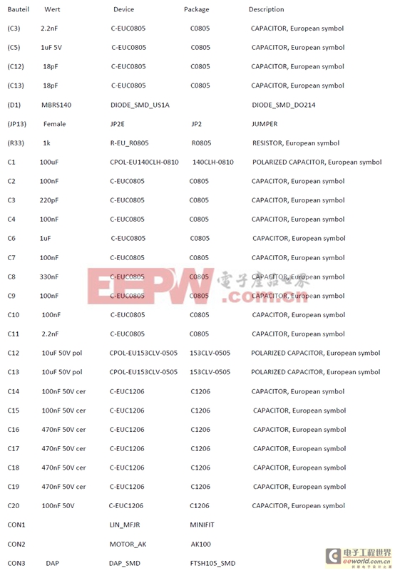
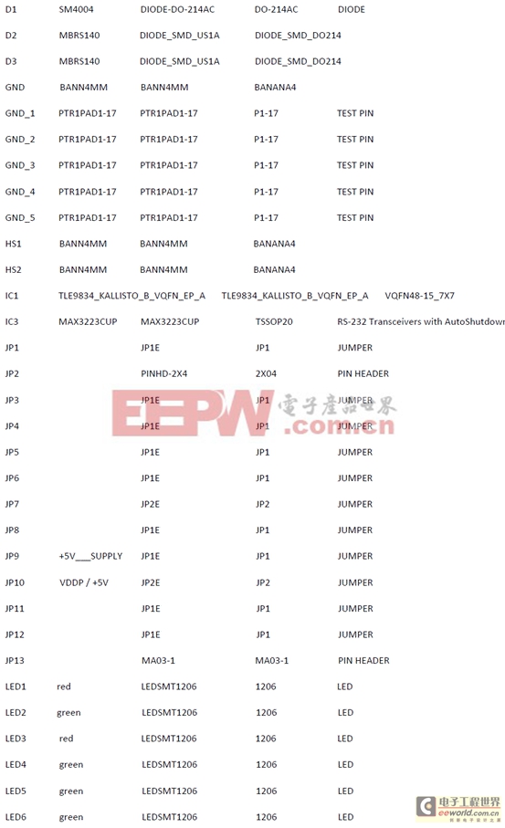
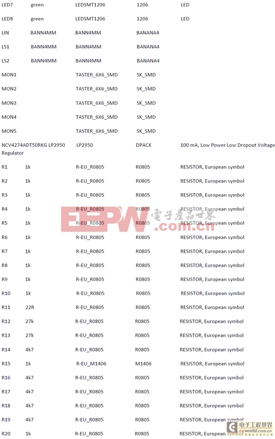
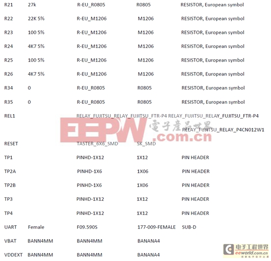
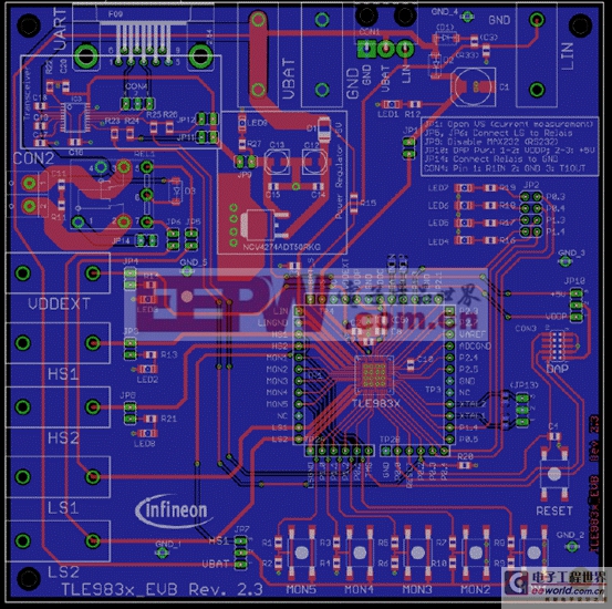
图6.TLE983x评估板PCB布局图(1)
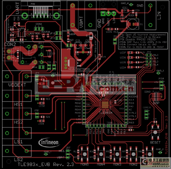
图7.TLE983x评估板PCB布局图(2)
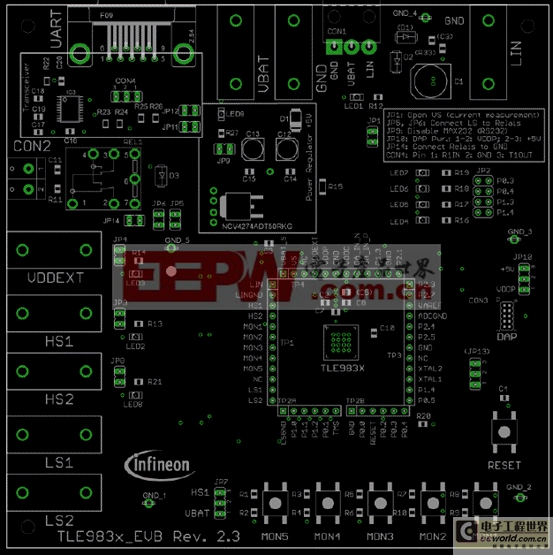
图8.TLE983x评估板PCB布局图(3)
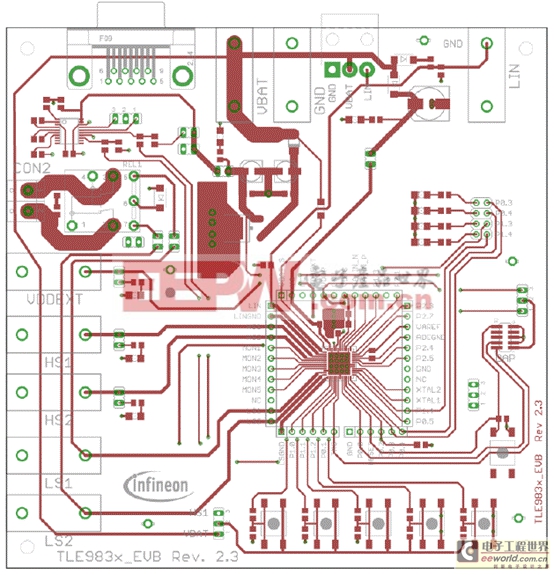
图9.TLE983x评估板PCB布局图(4)

图10.TLE983x评估板PCB布局图(5)
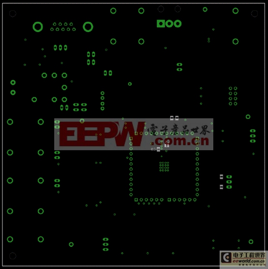
图11.TLE983x评估板PCB布局图(6)

图12.TLE983x评估板PCB布局图(7)

评论