一种基于FPGA 的驱动接口电路的设计

结合AD7862的转换速度, FPGA选择10MH z的处理时钟。对于整个转换过程的控制用一个状态机来完成, 状态机分为12 个状态( idle, convert1, busy1, reada1, w ait1, reada2,sw apchna,l convert2, busy2, readb1, w ait2, readb2), 其中idle状态为空闲等待转换状态; convert1指示第一次转换启动状态;busy1指示第一次转换状态; reada1状态下读取VA1; wait1状态为读取VA1和VA2之间的等待状态; reada2状态下读取VA2; sw apchnal状态指示交换到另一个通道进行转换;convert2指示第二次转换启动状态; 剩余状态和前面的类似,只不过是针对VB1 和VB2 而言。设计代码如下( 只描述VA1和VA2的部分, 剩下的类似):
process( clkdiv4, nrst)
beg in
if nrst = ‘0’ then
adc_state = id le;
e lsif( r ising _edge( clkd iv4) ) then
case adc_state is
when idle= >
ada0 = '0' ;
adconv = '1';
adncs = '1';
adnrd = '1';
clkcnt = 0;
if( start= ‘1’) then
adc_state = convert1;
end if;
w hen convert1= >
ada0 = '0';
adconv = '0' ;
if( adbusy= '1') then
adc_state = busy1;
end if;
w hen busy1= >
adconv = '1';
if( adbusy= '0') then
adc_state = reada1;
end if;
when reada1= >
if ( c lkcnt= 2) then
addataa1 = 0000 adda tain;
end if;
if( c lkcnt= 4) then
adc_state = w a it1;
adncs = '1';
adnrd = '1';
clkcnt = 0;
else
clkcnt = c lkcnt+ 1;
adncs = '0';
adnrd = '0';
end if;
when wait1= >
adc_state = reada2;
when reada2= >
if ( c lkcnt= 2) then
addataa2 = 0001 adda tain;
end if;
3设计电路的仿真验证
最终设计用Quartus 2 软件编译综合后在板上测试,FPGA 接口电路接受到的转换数据传给DSP芯片, 然后将DSP受到的数据用实时监控软件显示。图3是给AD 输入端加50 H z的正弦波信号(同时对其中三个输入端加信号), 监控软件显示的波形。
软件显示波形图
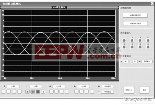
图3 软件显示波形图。
从图3波形图可以看出, 接口驱动电路成功的控制了AD7862芯片的采样过程, 从而验证了驱动电路设计的正确性。本文引用地址:https://www.eepw.com.cn/article/191398.htm


评论