PowerintTOP270VG100W小型反激电源解决方案

TOPSwitch-JX cost effectively incorporates a 725 V power MOSFET, high-voltage switched current source, multi-mode PWM control, oscillator, thermal shutdown circuit, fault protection and other control circuitry onto a monolithic device.
TOPSwitch-JX系列产品亮点:
EcoSmart – Energy Effi cient
• Ideal for applications from 10 W to 245 W
• Energy efficient over entire load range
• No-load consumption below 100 mW at 265 VAC
• Up to 750 mW standby output power for 1 W input at 230 VAC
High Design Flexibility for Low System Cost
• Multi-mode PWM control maximizes effi ciency at all loads
• 132 kHz operation reduces transformer and power supply size
• 66 kHz option for highest effi ciency requirements
• Accurate programmable current limit
• Optimized line feed-forward for line ripple rejection
• Frequency jittering reduces EMI fi lter cost
• Fully integrated soft-start for minimum start-up stress
• 725 V rated MOSFET
• Simplifi es meeting design derating requirements
Extensive Protection Features
• Auto-restart limits power delivery to 3% during overload faults
• Output short-circuit protection (SCP)
• Output over-current protection (OCP)
• Output overload protection (OPP)
• Output overvoltage protection (OVP)
• User programmable for hysteretic/latching shutdown
• Simple fast AC reset
• Primary or secondary sensed
• Line undervoltage (UV) detection prevents turn-off glitches
• Line overvoltage (OV) shutdown extends line surge withstand
• Accurate thermal shutdown with large hysteresis (OTP)
Advanced Package Options
• eDIP™-12 package:
• 43 W / 117 W universal input power output capability with
PCB / metal heat sink
• Low profi le horizontal orientation for ultra-slim designs
• Heat transfer to both PCB and heat sink
• Optional external heat sink provides thermal impedance
equivalent to a TO-220
• eSIP™-7C package:
• 177 W universal input output power capability
• Vertical orientation for minimum PCB footprint
• Simple heat sink mounting using clip provides thermal
impedance equivalent to a TO-220
• eSOP™-12 package:
• 66 W universal input output power capability
• Low profi le surface mounted for ultra-slim designs
• Heat transfer to PCB via exposed pad and SOURCE pins
• Supports wave or refl ow soldering
• Extended creepage to DRAIN pin
• Heat sink is connected to SOURCE for low EMI
TOPSwitch-JX系列典型应用:
• Notebook or laptop adapter
• Generic adapter
• Printer
• LCD monitor
• Set-top box
• PC or LCD TV standby
• Audio amplifi er
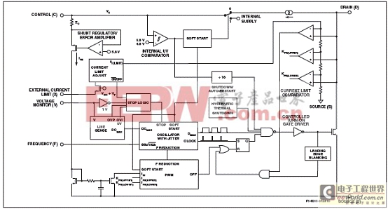
图1.TOPSwitch-JX系列方框图
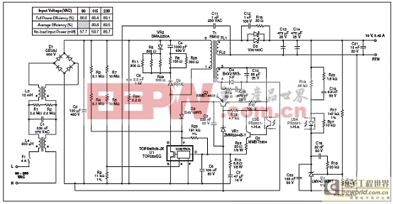
图2.TOPSwitch-JX系列通用输入19V 65W反激电源电路图
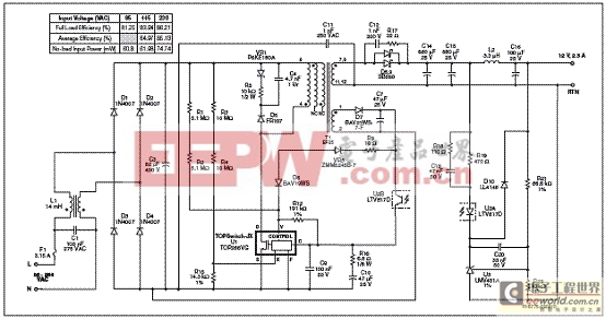
图3.TOPSwitch-JX系列通用输入12V 30W反激电源电路图
12V/24V 100W反激电源评估板
This document is an engineering report describing a 12 V / 24 V, 100 W flyback DC-DC converter utilizing a TOP270VG from the TOPSwitch-JX family of ICs. This power supply is intended for use in an LCD TV with LED back light. The board requires +380 VDC input, supplied from the PFC stage in a typical TV design.
100W反激电源评估板主要特性:
Highly energy efficient
Full load efficiency >90%
Efficiency >89% above 10% load
Average efficiency >90% (25%, 50%, 75%, 100% load points)
Simplifies meeting ENERGY STAR 2.0 and EuP requirements
Low cost, low component count and small PCB footprint solution
Performance met without synchronous output rectification
132 kHz operation optimized core size and efficiency performance
Low profile eDIP™-12 package for ultra-slim designs
Integrated protection and reliability features
Line under voltage lock out (UVLO)
Primary sensed output overvoltage shutdown (OVP). Latched OVP condition can be reset with a fast AC reset circuit.
Auto recovery output over current (OCP)
Meets limited power source (LPS) 100 VA requirement with a single point of failure
Accurate thermal shutdown with large hysteresis

图4.100W反激电源评估板外形图
100W反激电源主要指标:
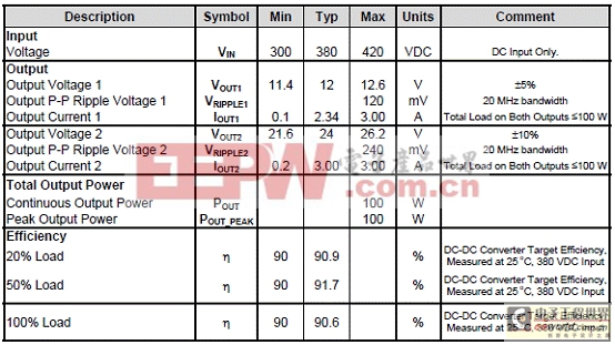
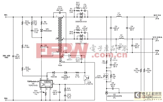
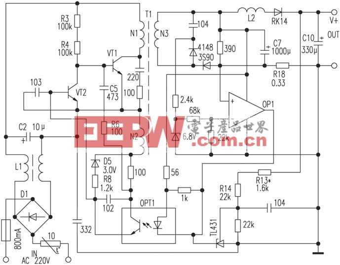
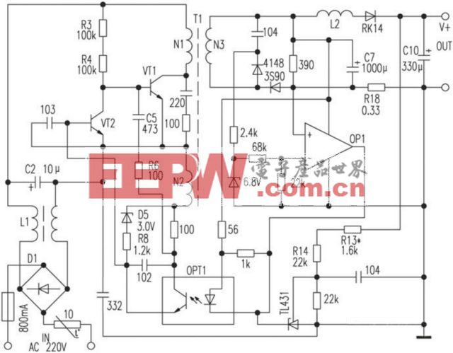
图5.100W反激电源评估板电路图
100W反激电源评估板材料清单(BOM):
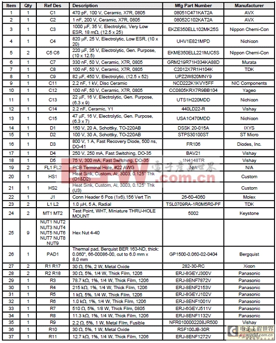
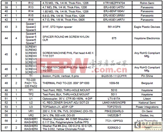
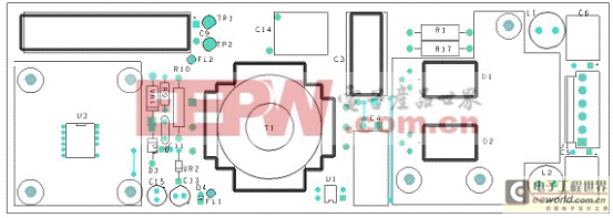
图6.100W反激电源评估板PCB布局图(顶层)
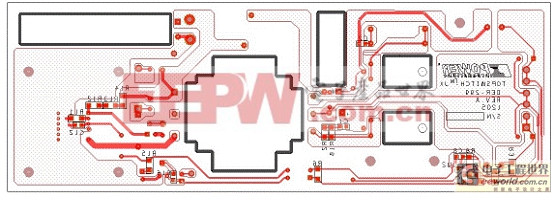
图7.100W反激电源评估板PCB布局图(底层)
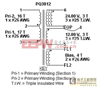
图8.变压器电路图
详情请见:
http://www.powerint.com/sites/default/files/product-docs/topjx_family_datasheet.pdf
和
http://www.powerint.com/sites/default/files/PDFFiles/der299.pdf

pwm相关文章:pwm是什么
电路图符号相关文章:电路图符号大全


评论