FPGA:SPI接口

SPI可以用作FPGA和其他芯片之间简单有效的通信方式。
本文引用地址:https://www.eepw.com.cn/article/202401/454461.htm
SPI 1 - 什么是SPI?
SPI是一个简单的接口,允许一个芯片与一个或多个其他芯片进行通信。
它看起来如何?
让我们从一个简单的例子开始,其中只有两个芯片必须一起通信。
SPI 需要在两个芯片之间使用 4 根线。
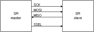
如您所见,这些电线被称为 SCK、MOSI、MISO 和 SSEL,其中一个芯片是“主芯片”,另一个芯片是“从芯片”。
SPI基础知识
基本上:
它是同步的。
它是全双工串行。
它不是即插即用的。
有一个(也只有一个)主站和一个或多个(或多个)从站。
更多细节:
同步:时钟由主机生成。
全双工串行:数据被串行化,在每个时钟周期内向每个方向传输一位数据,因此使用两条数据线(MOSI 和 MISO)。
非即插即用:主站和从站事先知道通信的细节(位顺序、交换的数据字长度等)。
一个主站:从站不能发起通信,只有主站可以。从属设备倾听并做出回应。
简单转移
假设主站和从站需要 8 位数据传输,首先传输 MSB。
以下是单个 8 位数据传输的样子。

MOSI线是“主输出”,而MISO是“从输出”。 由于SPI是全双工的,两条线同时切换,从主到从,从从到主,从到主。
更多细节:

主站下拉 SSEL 以向从站指示通信正在启动(SSEL 处于低电平有效状态)。
主机切换时钟八次,并在其 MOSI 线路上发送 8 个数据位。同时,它从MISO线路上的从站接收8个数据位。
主站向上拉 SSEL 以指示传输已结束。
如果主服务器有多个 8 位数据要发送/接收,则它只能在发送/接收完成后继续发送/接收并取消置位 SSEL。
多个从站
SPI主机可以通过两种方式与多个从机通信:并行连接大多数信号并添加SSEL线,或者通过链接从机。
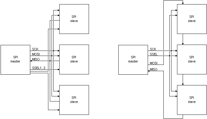
使用多 SSEL 线路技术时,一次只能激活一条 SSEL 线路,并且未选择的从站不得驱动 MISO 线路。
它有多快?
SPI可以轻松实现几Mbps(兆比特/秒)。 这意味着它可以用于未压缩的音频或压缩的视频。
SPI 2 - 简单的实现
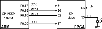
ARM 处理器
为了有机会测试我们新获得的 SPI 知识,我们使用了 Saxo-L 板。 它有一个 ARM7 处理器 (LPC2138) 和一个 Cyclone FPGA (EP1C3),通过 SPI 总线连接。
ARM 用作 SPI 主机,而 FPGA 用作 SPI 从机。 Saxo-L ARM 处理器实际上有两个 SPI 接口,一个称为 SPI0,另一个更高级的称为 SPI1/SSP。 它们都同样易于使用。我们在 Saxo-L 上使用 SPI1/SSP,因为它已预先接线在电路板上。

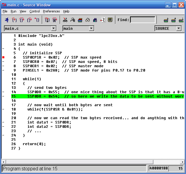
SPI 主机 - C ARM 代码
使用 SSP 只需初始化几个寄存器,然后写入/读取数据以自动发送/接收。
void main(void)
{
  // initialize SSP
  SSP0CPSR = 0x02;  // SSP max speed
  SSP0CR0 = 0x07;  // SSP max speed, 8 bits
  SSP0CR1 = 0x02;  // SSP master mode
  PINSEL1 = 0x2A8;  // SSP mode for pins P0.17 to P0.20

  while(1)
  {
    // send two bytes
    SSP0DR = 0x55;  // one nice thing about the SSP is that it has a 8-words deep FIFO
    SSP0DR = 0x54;  // so here we write the data to be sent without worrying

    // now wait until both bytes are sent
    while(!(SSP0SR & 0x01));

    // now we can read the two bytes received... and do anything with them
    int data1 = SSP0DR;
    int data2 = SSP0DR;
    // ...
  }
}
SPI 从机 - HDL FPGA 代码
现在是FPGA中的SPI从机。
由于SPI总线通常比FPGA工作时钟速度慢得多,因此我们选择使用FPGA时钟对SPI总线进行过采样。 这使得从机代码稍微复杂一些,但其优点是SPI逻辑在FPGA时钟域中运行,这将使以后的工作变得更容易。
首先是模块声明。
module SPI_slave(clk, SCK, MOSI, MISO, SSEL, LED);
input clk;
input SCK, SSEL, MOSI;
output MISO;
output LED;
请注意,我们有“clk”(FPGA 时钟)和一个 LED 输出......一个不错的小调试工具。 “clk”需要比 SPI 总线更快。Saxo-L 的默认时钟为 24MHz,在这里工作正常。
我们使用 FPGA 时钟和移位寄存器对 SPI 信号(SCK、SSEL 和 MOSI)进行采样/同步。
// sync SCK to the FPGA clock using a 3-bits shift register
reg [2:0] SCKr;
always @(posedge clk) SCKr <= {SCKr[1:0], SCK};
wire SCK_risingedge = (SCKr[2:1]==2'b01);  // now we can detect SCK rising edges
wire SCK_fallingedge = (SCKr[2:1]==2'b10);  // and falling edges
// same thing for SSEL
reg [2:0] SSELr;
always @(posedge clk) SSELr <= {SSELr[1:0], SSEL};
wire SSEL_active = ~SSELr[1];  // SSEL is active low
wire SSEL_startmessage = (SSELr[2:1]==2'b10);  // message starts at falling edge
wire SSEL_endmessage = (SSELr[2:1]==2'b01);  // message stops at rising edge
// and for MOSI
reg [1:0] MOSIr;
always @(posedge clk) MOSIr <= {MOSIr[0], MOSI};
wire MOSI_data = MOSIr[1];
现在,从 SPI 总线接收数据很容易。
// we handle SPI in 8-bits format, so we need a 3 bits counter to count the bits as they come in
reg [2:0] bitcnt;reg byte_received;  // high when a byte has been received
reg [7:0] byte_data_received;
always @(posedge clk)begin
  if(~SSEL_active)
    bitcnt <= 3'b000;  else
  if(SCK_risingedge)  begin
    bitcnt <= bitcnt + 3'b001;

    // implement a shift-left register (since we receive the data MSB first)
    byte_data_received <= {byte_data_received[6:0], MOSI_data};  end
    end
    always @(posedge clk) byte_received <= SSEL_active && SCK_risingedge && (bitcnt==3'b111);
// we use the LSB of the data received to control an LEDreg LED;
always @(posedge clk) if(byte_received) LED <= byte_data_received[0];
最后是传动部分。
reg [7:0] byte_data_sent;
reg [7:0] cnt;
always @(posedge clk) if(SSEL_startmessage) cnt<=cnt+8'h1;  // count the messages
always @(posedge clk)if(SSEL_active)begin
  if(SSEL_startmessage)
    byte_data_sent <= cnt;  // first byte sent in a message is the message count  else
  if(SCK_fallingedge)  begin
    if(bitcnt==3'b000)
      byte_data_sent <= 8'h00;  // after that, we send 0s    else
      byte_data_sent <= {byte_data_sent[6:0], 1'b0};
      end
      end
      assign MISO = byte_data_sent[7];  // send MSB first
// we assume that there is only one slave on the SPI bus
// so we don't bother with a tri-state buffer for MISO
// otherwise we would need to tri-state MISO when SSEL is inactiveendmodule
我们已经在 ARM 和 FPGA 之间建立了通信!
运行代码
当我们逐步执行 ARM 代码时,我们可以看到 LED 的状态发生变化,以及 FPGA 返回的数据。
现在让我们看看我们是否可以用SPI做一些有用的事情。
SPI 3 - 应用
LCD接口
由于我们已经知道如何驱动图形 LCD 面板,尤其是在文本模式下,让我们尝试从 LPC 中写出文本。
从FPGA的角度来看,LCD控制器使用几个blockram来保存字体,字符显示等... 因此,我们只需要确保SPI数据进入模块即可。
从ARM的角度来看,将数据发送到LCD模块的功能称为“SSP_WriteBlock”。
// function used to write in the LCD blockrams
void SSP_WriteBlock(char* ob, int len, int addr);

void LCD_PutString(char* s, int x, int y)
{
  // the blockram that holds the characters starts at address 0, and have 80 characters per line
  SSP_WriteBlock(s, strlen(s), x+y*80);
}

void main(void)
{
  SSP_init();

  LCD_PutString("Hello world!", 0, 0);
  LCD_PutString("FPGA4FUN.COM - where FPGAs are fun.", 4, 3);

  LCD_PutString("Char set:", 0, 7);
  int i; for(i=0; i<128; i++) LCD_PutChar(i, i, 8);

  LCD_Cursor_off();
}
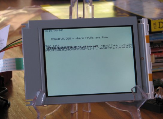
使用 LCD 控制器配置 FPGA 并运行 ARM 代码后,我们得到以下结果:


评论