MSL2164:16串LED驱动器设计指南详解(独家)

The MSL2164 and MSL2166 are highly integrated, flexible,16-string LED drivers that use external MOSFETs to allowhigh LED string currents and/or voltage. They include powersupply control to maximize efficiency and an advancedPWM dimming control circuit for regional dimming and 3DLED backlights. The drivers optionally connect to a videosubsystem to offer a simple architecture for use in LCD TVbacklight applications. Up to eight devices easily connecttogether to drive large numbers of LED strings in a system.
MSL2164引脚图:

MSL2164功能框图:
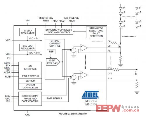
The drivers provide multiple methods of controlling LEDbrightness, through both LED regulation current control andthrough PWM dimming. Set the LED current to control colorand use pulse width control for brightness management andmotion blur reduction. An on-chip EEPROM stores all thedefault control register values, which are applied at start-upand reconfigured through the serial data interface.
MSL2164时序图:

The MSL2164/MSL2166 interface to a microcontroller or FPGA via SPI. The 20MHz bus addressable SPI interfacesupports up to eight devices per Chip Select line. LED PWMdimming is internally generated and synchronized to thevideo VSYNC and HSYNC signals or directly controlled by anexternal PWM drive signal applied to the PWM input. Theyalso feature phase spreading when external PWM dimming,with a progressive 1/16 phase delay per string to reduceLED power supply transient load and reduce power supplyinput capacitor size.
PWM dimming is either synchronized to an external signalapplied to PHI, generated from the internal oscillator forstand-alone applications or set directly by a signal at thePWM input. For video systems, derive the PHI signal fromVSYNC. A 1x to 32x frequency multiplier processes PHIfor PWM dimming at multiples of the video frame rate.
Individually program each string’s “on” time with up to 12-bitresolution when using the integrated PWM generator. Thefinal PWM dimming resolution depends upon the ratio of theprocessed GSC to processed PHI frequencies, because the“on” time is an integer number of GSC clock cycles between0 and 4095, and is scaled by the value of the 12-bit globalintensity register. Phase delay is also an integer number ofprocessed GSC clock cycles, to synchronize timing to thevideo frame. An on-chip frequency multiplier is provided inorder to fully utilize the 12-bit dimming range. The “on” timecount can be further scaled by a 12-bit global intensity value.
The processed GSC signal (the signal after being frequencymultiplied or divided, from either internally or externallygenerated signal at GSC) precisely sets each string’s phasedelay so that it is synchronized to its physical position onthe LCD panel, relative to the beginning, middle or endof the video frame. There are four different types of PWMmodulation modes, each defined by the part of the “on”time or off-time set by the PHDLYn[11:0] register (part of theSTRnSET register). The modes are “forward,” “center,” “reverse,” and “inverse”. All four modes use the PHDLYnregister to set the defined edge, and PWMn[11:0] to setthe “on” time as a number of processed GSC pulses.
Thefour different modes and register definitions are illustratedin the figure below, showing the current waveforms. Thedelay for string 0 is held at 0, and the PWM width is thesame for both strings and all the modes. Datan in thefigure refers to both the dimming data and the phase delaydata presented for the nth frame. For “forward” modePHDLYn specifies the number of processed GSC cyclesafter the processed PHI edge that the string “on” timebegins and the PWMn register specifies the “on” time.
In this mode the falling edge varies with the “on” timewidth programmed in the PWMn register, with the risingedge held constant. In “center” mode, the delay is setfrom the processed PHI edge to the center of the PWM onpulse with width set by the PWMn register. Both the risingand falling edge vary based on the PWMn with the centerheld constant within a processed GSC cycle. In “reverse”mode, the PHDLYn sets the delay from the next frame’sprocessed PHI edge to the falling edge of the PWM “on”time and the PWMn register determines the PWM “on”time. Therefore the rising edge varies with PWMn and thefalling edge is held constant. In “inverse” mode, the delayis set from the next frames PHI edge backwards to thefalling edge of the “on” time. The rising edge varies withthe PWMn register, while the falling edge is held constant.
相关阅读:
最实用的LED驱动设计的18个经典案例分析,原理,电路,方案,验证,一网打尽
推荐阅读:
1.MSL2164:16串LED驱动器应用案例精讲
摘 要:这些LED驱动器可与爱特梅尔tinyAVR®、megaAVR和AVR XMEGA等AVR®微控制器(MCU) 无缝集成。微控制器处理定时和调光指令,将数据发送给MSL2164和MSL2166器件。 AVR器件与固件提供优化整个背光设计的总体解决方案,提供相比竞争解决方案更卓越的性能。


评论