Building a DC-DC power supply

Also see:
- Application note 2031, "DC-DC Converter Tutorial"
- Power Supply Cookbook
Introduction
A designer's first DC-DC converter circuit generally has one thing in common with first attempts in any other field: it has a slim chance of working satisfactorily when first powered. That may sound like a gloomy assessment, but it nevertheless reflects the realities of switch-mode power-supply design. DC-DC converters are complex systems. Even when simplified by highly integrated ICs, they still require extensive component calculations and thoughtful selection of the controller IC. In addition, they are sensitive to board layout and component parasitics (i.e., the characteristics of a component that are not ideal, such as resistance in a capacitor or capacitance in a MOSFET switch).There are few comprehensive sources of DC-DC design information. Engineering textbooks discuss control theory, loop compensation, and other highly detailed analytical methods. Data sheets for DC-DC converters give specific formulas and some layout information. Less information is available to guide the overall design of integrated-circuit-based DC-DC converters from start to finish.
This article fills in information gaps for a first DC-DC power supply design. It is the result of the author's failures and successes with scores of power-supply circuits.
Device selection
Once the initial specs of a DC-DC design are selected (e.g., input voltage range, output voltage, output current), the first step is to select a converter IC. The desired DC-DC topology will narrow this choice. If the input voltage is greater than the output voltage, choose a buck (i.e., step-down) topology. If the input voltage is less than the output voltage, choose a boost (i.e., step-up) configuration. If the input voltage ranges above and below the output voltage, a buck-boost converter or a SEPIC converter is needed. Lastly, if the output voltage is negative, an inverting topology is used.Note that a boost DC-DC converter output will rise with input voltage when the input exceeds what has been set for the output voltage. Similarly, a buck converter cannot provide the desired output when the input voltage is less than that output. It is said to be "in dropout" when that happens.
Many DC-DC load requirements can be met by DC-DC converter ICs that include integral power switches. Most such ICs include MOSFETs, but some employ bipolar transistors. The load current capability of newer internal MOSFET DC-DC ICs can handle up to 25A (e.g., theMAX8655andMAX8686). An internal-switch device, if available, is usually preferred, both for overall simplicity and (often) for lower total cost.
High-power or high-voltage applications that exceed the abilities of internal-MOSFET devices will need external MOSFET switches. DC-DC converters designed for driving external power switches are usually called "controllers." These ICs include drivers for quickly charging and discharging an external MOSFETs' gate capacitance. The ability to quickly charge and discharge a MOSFET gate is critical in achieving high-efficiency conversion. The switch wants to spend as little time as possible in transition between its on and off states because that is when power loss is greatest. Most DC-DC controllers specify a maximum gate capacitance that they can drive. (See the section, MOSFET gate capacitance below.)
In addition to topology, voltage, and current considerations, there are likely to be other application characteristics that direct the choice of DC-DC IC. For example, in most automotive applications a DC-DC converter should be able to tolerate cold-crank and load-dump conditions as well as a -40°C to +125°C temperature range. Maxim's on-line parametric search tool helps choose among converter features and specifications.
MOSFET gate capacitance
Power MOSFET manufacturers provide various dynamic and switching parameters on their data sheets in addition to DC specs like on-resistance. In most cases, when using external MOSFETs with DC-DC converters, total gate charge (QG) is of primary interest. Choose MOSFETs for which the QGis within the range recommended by the manufacturer of the DC-DC converter. Using the MOSFET's typical QGvalue is fine for most cases. The maximum number is usually overly conservative. The QGspec is used when driving an "open-drain" low-side n-channel or high-side p-channel MOSFET, or in other words, when the MOSFET source does not change voltage during switching.In circuits where the source voltage does change during switching, the more useful dynamic parameter is reverse transfer capacitance (CRSS). CRSSis used in calculating switching loss in a high-side n-Channel MOSFET of a buck converter in accordance with the following equation:
PD(switching) = (CRSS× VIN(MAX)² × fSW× ILOAD)/IGATEWhere IGATEis the peak gate source and sink current, and fSWis the switching frequency.
PWM and other control schemes
The most popular DC-DC converter control scheme is pulse-width modulation (PWM). PWM converters maintain a constant switching frequency over a broad range of loads. That behavior can be important when switching noise might interfere with other processes in a system. Confining the noise to a known band often mitigates interference.The next most common control scheme is pulse-frequency modulation (PFM), where the converter supplies switching pulses only when required by the load. PFM converters excel in applications that require low quiescent current and high efficiency at very small loads. Some converters ICs employ both schemes to combine good idle-mode efficiency with low noise.
The switching frequencies of IC DC-DC converters and controllers range from 65kHz to over 4MHz. In general, it is probably best to avoid devices that operate below 100kHz, as such frequencies are typical of old devices with poor efficiency. Higher switching frequency allows smaller external components along with lower peak currents and I²R losses, but core losses, gate-charge currents, and switching losses increase. (See the section on High-switching frequency reduces component size.) If the application demands the smallest possible size, then look for converters with switching frequencies at 1MHz and above. Otherwise, simply choose a device that meets the power criteria and verify that its switching frequency does not interfere with other components in the system.
High-switching frequency reduces component size
A continuous trend in DC-DC converters is to higher switching frequencies in order to achieve smaller component sizes. When more switching cycles occur per second, the energy per switching cycle (and the size of the components that store that energy) can be smaller. Inductor values, for instance, can be lower. Inductor behavior is governed by the following equations:VL= L × (di/dt)For example, consider a buck converter operating at 500kHz with a 10µH inductor. Changing the frequency to 1MHz allows exactly one-half the inductance, or 5µH, to be used to achieve the same power transfer. Although the inductance value decreases by one-half, the current requirement remains the same. The second equation shows that we just reduced the inductor's required energy storage by half as well. Since inductance is proportional to the square of the number of turns, reducing inductance by half means the turns count is reduced to 70.7% of the original number. Reducing the turns also proportionally lowers the DC resistance (DCR), so the resulting inductor is smaller and has lower DCR.
WL= (L × i²)/2
Higher switching frequency also reduces the size of the output capacitor. In the example above, the capacitance required is 67µF at 500kHz, but only 33µF at 1MHz. The ripple-current specification remains unchanged.
After choosing a particular device type (buck, boost, etc.), make the final selection by consulting DC-DC converter manufacturers' websites. Always check the manufacturer's website for the latest data sheet. While there, look for application notes that apply to the device that you are considering. They serve as a guide and often include circuits that can be used with little or no modification. (See: Power Supply Cookbook, Maxim's power supply application notes, and the power and battery-management products.)From application notes and data sheets you can obtain the equations that govern the design for your device.
Design equations
DC-DC converter data sheets should contain equations helpful for designing your circuit. Macro models or spreadsheet files for calculating component values may also be available on the product webpage. Be sure to read the IC data sheet carefully to ensure that you select the proper equations for the required performance and operating mode. Once the major design parameters are known and you have the right equations, the best tool for evaluating the equations is a spreadsheet such as Excel® or an engineering-math program such as MathCAD. Maxim's EE-Sim® tool generates an interactive schematic that features a highly efficient simulation engine. If the selected device has an EE-Sim model, use that to calculate the appropriate components for your design.Spreadsheet calculations
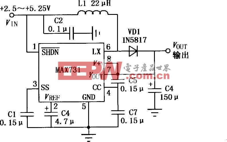
Spreadsheets are an effective basic design tool for DC-DC converters. They can even serve as crude circuit simulators, and their "Solve" feature can help optimize component values. When used with DC-DC converter equations, a spreadsheet allows an iterative approach that aids component selection by quickly indicating cause-and-effect relationships.As an example, consider the MAX1742, an internal-switch buck converter. The data sheet's Design Procedure section gives necessary information and the order for calculations. We assume a constant 5V input, a 3.3V output with maximum load current of 500mA, and a 500kHz operating frequency.
Use the defined variable names whenever possible. As you enter more equations, define the results of those calculations with more names. Choose the names so you can easily remember what they mean when you check the calculations later.
First, across the top of a new worksheet, enter names for all predetermined values (Figure 1). These names might include VINMIN, VINMAX, VOUT, IOUT, FREQ (frequency), and other terms associated with the converter. In the cells immediately beneath the cells containing those names, define cell names to match the names typed above.
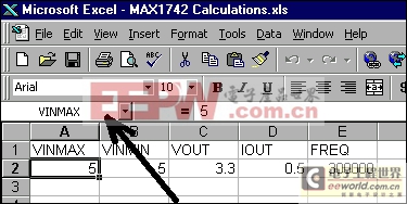
Figure 1. Using cell names in spreadsheets.
To define a cell name: select the cell to be named, go to the Insert menu and select Name, then Define on the submenu. In Excel, a dialog box pops up to suggest (as a default name) the text immediately above the selected cell. To name the cell, click OK on this dialog box. Proceed across the row until all these fields have been named. This naming procedure allows you to refer to VINMAXin your calculations instead of cell A2. Note that the selected cell in Figure 1 is A2, with a value of 5. The cell's name is indicated just above the row labeled A. Next, scan through the design procedure and pick all the required component values (Table 1). Note that original spreadsheet values have been converted to SI units for clarity.
Table 1. Initial component calculations
| VINMAX | VINMIN | VOUT | IOUT | Frequency |
| 5 | 5 | 3.3 | 0.5 | 500kHz |
First calculate RTOFF.
| VPMOS | VNMOS | tOFF | RTOFF |
| 45mV | 35mV | 673ns | 66.3kΩ |
Choose the value for LIR, then calculate L and IPEAK.
| LIR_INIT | L | IPEAK |
| 30% | 14.8µH | 575mA |
Next the output capacitor parameters are calculated.
| IRIPPLE | ESR_MIN | COUT_MIN |
| 529.6mA | 0.22Ω | 6.73µF |
Soft-start calculations
| tSS | CSS |
| 100ms | 0.22µF |
Component selection
Using values from Table 1, select the DC-DC converter's peripheral components. Check the data sheet recommendations to ensure each component's suitability for the task. If the calculated inductor value is not available, choose the next smaller standard value. If a calculated capacitor value is not available, choose the next larger standard size.The inductor is selected primarily based on inductance value, DC resistance (DCR), and the peak-current requirement. Also make sure that the inductor is designed to operate at the desired switching frequency. If that data is not provided, choose another inductor for which the data is available. Inductors are available in surface-mount and through-hole versions, but in general surface-mount types offer better performance, particularly at high switching frequencies. In our example we have a close match with a Coiltronics® Thin-Pac TP1-150, a 15µH inductor with 0.73A saturation current.
The input capacitor reduces both peak current drawn from the input supply, and radiated noise to other elements of the system. Most data sheets either suggest specific values or give equations for calculating the input capacitor value. Make sure that the capacitor is specified with a ripple-current rating near the selected switching frequency. For our 500kHz example, the capacitor could be an organic electrolyte, organic polymer, ceramic, or tantalum type.
Tantalum capacitors can respond violently to large instantaneous voltage steps and high current surges so do not use tantalum for input bypassing where input power will be connected through a mechanical switch. Our circuit input is from a regulated supply, so we need not worry about that limitation. We therefore select a capacitor that meets the ripple-current rating and voltage requirements, such as an AVX® TPS series 100µF capacitor in the C size case and rated for 10V and 742mA ripple current. The input-capacitor ripple current in a step-down converter can be approximated as:
IRIPPLE_CIN (RMS)= [IOUT/VIN][VOUT(VIN- VOUT)]-1/2As a starting point, choose a capacitor that meets the recommended minimum value of 22µF and verify that it meets the required voltage rating. For our example, the AVX TPS series 33µF capacitor in the C size case is rated for 10V operation. Its maximum ESR is 0.375Ω, which is close to the target.
The soft-start capacitor and the tOFFresistor have no special requirements; select them from the closest available standard values. To complete component selection, choose the remaining values from a typical application circuit or the evaluation (EV) kit schematic.
Spreadsheet revisited
Because capacitors and inductors come in a finite number of standard values, the closest available value can differ from the calculated value by more than 20%. In that case, the spreadsheet should be recalculated with actual values to verify that the circuit still meets its design objectives. As shown inTable 2, further corrections are not necessary because our RTOFFand inductor choices have a minimal impact on the circuit's operating point.Table 2. Checking actual component values
| Calculate tOFFand frequency using selected RTOFFvalue. | ||
| RTOFF | tOFF | Frequency |
| 68kΩ | 688ns | 488.8kHz |
| Calculate LIR and IPEAKusing selected L value. | ||
| L | LIR | IPEAK |
| 15µH | 30.3% | 576mA |
Component placement
When laying out the PCB for this example, you should first place the DC-DC converter IC (e.g., the MAX1742), the inductor, and the input and output capacitors. Then, move those components so the input capacitor is close to the MAX1742's input pins; the inductor is close to the IC's LX pin; and the output capacitor is close to the inductor and the IC's ground pins. Optimizing all of these component positions may require compromises, depending on the IC pin locations. In Maxim's DC-DC converter ICs, pin locations are carefully selected for circuit performance and ease of PCB layout.The most critical node in most cases is the common ground between the input and output capacitors and the ground pin of the IC. These three grounds must be very close, usually within 10mm of each other (Figures 2aand2b). During the charge cycle (Figure 2a), current flows from the input capacitor through the high-side switch, inductor, output capacitor, across the ground plane, and back into the input capacitor. During the discharge cycle (Figure 2b) current continues to flow through the inductor, output capacitor, across the ground plane, back through the IC's ground pin, through the low-side switch, and back into the inductor.
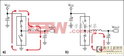
Figure 2. These diagrams illustrate current paths during step-down DC-DC converter's charge (a) and discharge (b) cycles.
Because this circulating current can interfere with other circuits, its path length must be kept short (Short paths also contribute to stable operation and efficiency). Too long a path length in the ground portion (during either cycle) can compromise the circuit's reference for other circuit elements. That condition can also lead to poor regulation, excessive output ripple, and even instability. Placing the input capacitor ground, output capacitor ground, and IC ground adjacent to each other minimizes those unwanted effects.
Another important consideration for the ground connections of current-carrying components is to use multiple parallel PCB vias if the ground plane is on another PCB layer. This is especially important for input and output filter capacitors. A single via often adds resistance and inductance in series with the capacitor, reducing its effectiveness.
Power ground
After placing components according to the criteria above, the common ground is connected either with wide traces or with a polygon of solid copper. Use as much copper as possible to create a low-impedance path between the elements.Local ground
The typical application circuit for many DC-DC converter ICs indicates multiple symbols for ground—this is an excellent hint on how to accomplish a successful circuit layout. One of the different symbols often indicates a local ground plane and is typically titled SGND or AGND. Elements that connect to the local ground plane can include reference-bypass capacitors, resistor-dividers, and resistors that set operating points (such as resistor RTOFFin the example), but should not include high-current grounds such as those from switch MOSFETs.The local ground plane is a solid copper polygon best tied to the power ground plane atone pointonly, typically the pin titled PGND. Local ground planes prevent switching currents from polluting the low-noise local ground plane. Those switching currents often exceed 10A.
Ground plane
Because many systems rely on a separate ground plane for all components on the PCB, it is often tempting to use the ground plane of the DC-DC converter section for that purpose.That temptation should be avoided.The switching currents mentioned above can cause ground glitches across the board, produce excessive EMI, cause invalid logic states, raise the noise level, and cause instability. The proper interface between DC-DC converter circuitry and the ground plane is a single via (or a small grouping of multiple vias), leading from the poured copper power ground to the buried ground plane.Signal routing
After completing the initial ground layout, make the required connections for the first four critical components and then place and route the remaining components. A useful approach is to take all noncritical signals to the backside of the PCB with small vias while reserving the top side of the board for the routing of critical high-current traces.When routing nonpower traces on circuit boards, consider the DC and AC components of the signal. Remember that every trace is a resistor and an inductor, and may also capacitively couple to other traces. Each signal's use in the circuit determines the optimal trace width and length. High-speed and high-current signals demand short, wide traces. Longer, thinner traces are acceptable for less critical signals such as low-speed logic. Route high-speed switching nodes away from sensitive analog areas like the compensation network and feedback node. Also keep the compensation and feedback networks as small as possible to prevent noise pickup. When provided, refer to the layout and grounding guidelines on the PCB layout of the EV kit for more help.
Verification
After the converter is completed, and prototype boards assembled, the overall design should be verified for performance to the original criteria. If the design was implemented diligently with regard to the issues discussed, chances for initial success are good. But even conscientious designs may still require "tweaking." When making changes, verify with calculations or models to be sure that some other important characteristic is not being compromised. For example, you may determine that output ripple is acceptable with smaller output filter capacitance, but such a change might also impact stability.Efficiency
Efficiency is often a key DC-DC converter performance parameter, particularly for devices operating from a battery, and especially so for power supplies in laptop computers and small handheld equipment. Laptop power-supply efficiency directly affects battery life, but it also impacts power dissipation; it should be coordinated with the heat-removal limitations. Note that a DC-DC converter supplying 50W at 85% efficiency still dissipates 8.8W of heat inside the case.In laptops, efficiency is important over a wide range of operating conditions. Examples include low battery, full battery, and battery charging under both standby and operating states. In other applications, the efficiency-critical points depend on how the device is used. Light-load efficiency and quiescent operating current can be most important in small handheld device like a personal glucose meter, while full-load efficiency and heat generation are most critical in network hardware.
Load regulation
A converter's ability to stay within the specified output-voltage tolerance, regardless of load, is called load regulation. It applies at DC, but it also includes fast transients such as those encountered with high-speed CPUs. You should verify that the output voltage stays within specification when loaded with currents ranging from zero to the maximum. Ensure that the output voltage does not undershoot its minimum value when the load changes quickly from minimum to maximum. Ensure that it does not exceed its maximum value when the load current drops from maximum to minimum. Note that the line- and load-regulation specs quoted in most data-sheet electrical characteristics tables are measured at DC, while transient performance is usually shown in the typical operating curves. For more information, see application notes 752, "Creating a fast load transient," and 3453, "Testing a power supply for line and load transients."Line regulation
A power supply's ability to maintain output-voltage regulation with a varying input voltage is called line regulation. Again, it should be examined both at DC and with a fast AC transient. A transient is encountered when a laptop computer switches from its AC adapter supply to its internal battery and back. In some systems, the voltage change can be as large as 10V. Verify that the output voltage stays within specification when the input voltage changes from minimum to maximum. Make sure that step changes in the input voltage do not cause peaks or valleys in the output voltage that exceed the output-voltage specifications.Temperature sensitivity
It may be convenient to evaluate a system on a lab bench and judge it ready for the application, but one more critical condition needs examination: performance over the worst-case operating-temperature range. Performance to the electrical criteria above should be measured at the highest and lowest temperatures that the system will encounter during operation. Watch for parameters that change drastically and those that approach upper or lower limits over temperature.The best way to evaluate a system over temperature is to use an environmental chamber. The chamber lets you conduct computer-controlled experiments over a broad range of temperatures and with an accuracy of 1°C or better. In cases where a chamber is not possible, you can still get an idea of overtemperature performance with less sophisticated equipment. Common heat guns and even hairdryers are useful in heating a circuit while under test. To cool a circuit well below ambient temperature, spray it with a compressed inert gas cold spray (offered in many technical catalogs). When cooling components, avoid condensation. If condensation does occur, understand that a circuit fluctuation might be due to moisture on the circuit board and not circuit sensitivity to temperature.
Conclusion
DC-DC power-supply design is neither rocket science nor common knowledge. The list of characteristics that need to be addressed in a successful design may seem daunting, but a methodical approach can result in a working circuit with minimal iteration. By applying the principles in this article, you can eliminate most of the typical first-design missteps.Maxim offers EV kits for most of its DC-DC converters. Maxim's free EE-Sim simulation tool can also be used for more reliable power supply designs, and is available for a growing number of power supply devices.


评论