PWM-controlled 4C20mA transmitter is galvani

A similar version of this article appeared in the February 24, 2009 issue of EE Times magazine.
The accuracy of a 4C20mA transmitter depends on the integrity of its current-loop path, which must be free of shunt paths and ground loops―both within the transmitter and external to it. External to the transmitter are spurious paths in the outside loop wiring and its power supply. Internal to the transmitter, shunt paths and ground loops are usually created at the point where you insert a control signal into the transmitter circuitry. To eliminate errors introduced by possible spurious current paths, the signal must be DC coupled with full galvanic isolation yet inserted with accuracy.
The circuit of Figure 1 comprises a loop-powered 4C20mA precision transmitter (MAX4236, BSP149, and MAX6138A) with large-compliance output stage, and a precision PWM signal coupler with galvanic isolation from the PWM signal source.
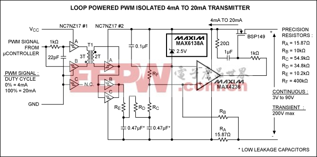
Figure 1. This loop-powered 4C20mA transmitter features PWM drive and galvanic isolation from the input signal.
The external PWM-encoded signal is a rectangular waveform generated by a microcontroller or PWM modulator, and is usually produced by a control algorithm run by the microcontroller from a sensor output or other analog-command level. The input-signal duty cycle represents the original signal as a percentage of an arbitrary reference. In this case, the PWM-coupler values are adjusted so a 0% duty cycle corresponds to 4mA from the transmitter, and a 100% duty cycle corresponds to 20mA.
Sections A and B of the NC7NZ17#1 (a TinyLogic UHS triple buffer with Schmitt-trigger inputs) form a bipolar edge detector that applies a short 20ns pulse to the 3-turn primary of transformer T1. The polarity of this pulse depends on the sign of the input edge being detected.
At the secondary of T1, the pulse sets or resets the flip-flop formed by buffer #2A and the secondary, thereby replicating the input signal at the output of #2A. T1 is a 3-to-2-turn transformer built around a Fair-Rite ferrite core, type 2673000101. Its small size (3.5mm in diameter and 3.25mm in length) yields 1pF of capacitance at the primary and secondary. The maximum voltage it can withstand depends on the wire insulation used and the way T1 is mounted.
The two remaining buffer sections (B and C) are connected in parallel with their inputs attached to the flip-flop output. Their outputs produce a precision signal whose duty cycle replicates that of the input signal, yet provides precise and stable low/high values―thanks to the CMOS output that tracks the rail voltages exactly, and to the precision reference (MAX6138A) that serves as the transmitter power supply.
The paralleled buffer outputs drive a low-pass filter whose output is the average of the reconstituted PWM input signal, referred to the value of the transmitter supply voltage (the 2.5V precision reference). This average value is a stable and very linear analog of the input signal's duty cycle. Fast propagation in the coupler ( 30ns H
 L and L H), and its small skew ( 2ns) ensure that negligible nonlinearity is introduced by the digital part of the coupler. The recovered average value drives the transmitter output, producing 4mA at 0% duty cycle and 20mA at 100%. For PWM input frequencies in the range 500Hz to 50kHz, the circuit operates with less than 0.1% coupler insertion error.
After power-up, power-loss, or loss of input signal, the Figure 1 circuit's output state can remain undetermined until after the next input transition edge. The circuit of Figure 2 removes that ambiguity with an input-transitions loss detector. When triggered by an interval of approximately 3ms with no transitions, it connects the transmitter directly to the output of an optocoupler. The optocoupler senses the state of the input line at which it is resting, and imposes that state on the output current. That is, H state = 100% duty cycle
20mA, and L state = 0% duty cycle 4mA. Reasons for not using the optocoupler for PWM coupling include its much longer propagation time, and its large, temperature-dependent propagation skew at any reasonably low levels of supply current.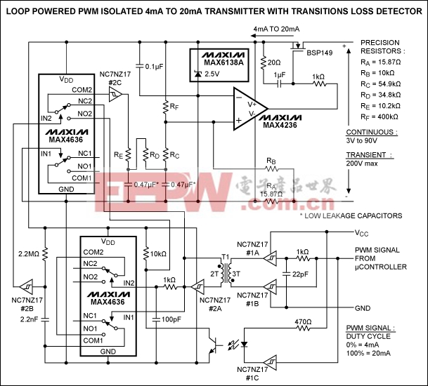
Figure 2. Adding a transitions-loss detector to the Figure 1 circuit eliminates the brief output uncertainty that can accompany a power-up, power-loss, or loss of input signal.
The transitions-loss detector of Figure 2 consists of two analog switch ICs (MAX4636). The one in the lower half of the circuit discharges a 2.2nF capacitor with every cycle of input signal. If a time interval longer than 3ms elapses without a transition, the capacitor charges to a level that fires the Schmitt-trigger input of buffer #2B. In turn, this buffer drives the second analog switch (upper half of the circuit) to switch the input of buffer #2C from the PWM output of the coupler to the optocoupler output, thereby replicating the (now static) input line.


评论