Virtex-6 FPGA ML605开发评估技术方案

Virtex-6 FPGA适合用有线通信,无线基础设备和广播设备等领域.本文介绍了Virtex-6 FPGA主要特性,以及骨干网OTU-4成帧与EFEC框图, LTE 2x2无线电设计框图和支持SD/HD/3G-SDI接口的新一代交换框图, Virtex®-6 FPGA ML605评估套件主要特性和详细电路图.
本文引用地址:https://www.eepw.com.cn/article/151880.htmThe Virtex®-6 family provides the newest, most advanced features in the FPGA market. Virtex-6 FPGAs are the programmable silicon foundation for Targeted Design Platforms that deliver integrated software and hardware components to enable designers to focus on innovation as soon as their development cycle begins. Using the third-generation ASMBL (Advanced Silicon Modular Block) columnbased architecture, the Virtex-6 family contains multiple distinct sub-families. This overview covers the devices in the LXT, SXT, and HXT sub-families. Each sub-family contains a different ratio of features to most efficiently address the needs of a wide variety of advanced logic designs. In addition to the high-performance logic fabric, Virtex-6 FPGAs contain many built-in system-level blocks. These features allow logic designers to build the highest levels of performance and functionality into their FPGA-based systems. Built on a 40 nm state-of-theart copper process technology, Virtex-6 FPGAs are a programmable alternative to custom ASIC technology. Virtex-6 FPGAs offer the best solution for addressing the needs of high-performance logic designers, high-performance DSP designers, and high performance embedded systems designers with unprecedented logic, DSP, connectivity, and soft microprocessor capabilities.
Virtex-6 FPGA 主要特性:
Three sub-families:
Virtex-6 LXT FPGAs: High-performance logic with advanced serial connectivity
Virtex-6 SXT FPGAs: Highest signal processing capability with advanced serial connectivity
Virtex-6 HXT FPGAs: Highest bandwidth serial connectivity
Compatibility across sub-families
LXT and SXT devices are footprint compatible in the same package
Advanced, high-performance FPGA Logic
Real 6-input look-up table (LUT) technology
Dual LUT5 (5-input LUT) option
LUT/dual flip-flop pair for applications requiring rich register mix
Improved routing efficiency
64-bit (or two 32-bit) distributed LUT RAM option per 6-input LUT
SRL32/dual SRL16 with registered outputs option
Powerful mixed-mode clock managers (MMCM)
MMCM blocks provide zero-delay buffering, frequency synthesis, clock-phase shifting, inputjitter filtering, and phase-matched clock division
36-Kb block RAM/FIFOs
Dual-port RAM blocks
Programmable
- Dual-port widths up to 36 bits
- Simple dual-port widths up to 72 bits
Enhanced programmable FIFO logic
Built-in optional error-correction circuitry
Optionally use each block as two independent 18 Kb blocks
High-performance parallel SelectIO technology
1.2 to 2.5V I/O operation
Source-synchronous interfacing using ChipSync technology
Digitally controlled impedance (DCI) active termination
Flexible fine-grained I/O banking
High-speed memory interface support with integrated write-leveling capability
Advanced DSP48E1 slices
25 x 18, two’s complement multiplier/accumulator
Optional pipelining
New optional pre-adder to assist filtering applications
Optional bitwise logic functionality
Dedicated cascade connections
Flexible configuration options
SPI and Parallel Flash interface
Multi-bitstream support with dedicated fallback reconfiguration logic
Automatic bus width detection
System Monitor capability on all devices
On-chip/off-chip thermal and supply voltage monitoring
JTAG access to all monitored quantities
Integrated interface blocks for PCI Express® designs
Compliant to the PCI Express Base Specification 2.0
Gen1 (2.5 Gb/s) and Gen2 (5 Gb/s) support with GTX transceivers
Endpoint and Root Port capable
x1, x2, x4, or x8 lane support per block
GTX transceivers: up to 6.6 Gb/s
Data rates below 480 Mb/s supported by oversampling in FPGA logic.
GTH transceivers: 2.488 Gb/s to beyond 11 Gb/s
Integrated 10/100/1000 Mb/s Ethernet MAC block
Supports 1000BASE-X PCS/PMA and SGMII using GTX transceivers
Supports MII, GMII, and RGMII using SelectIO technology resources
2500Mb/s support available
40 nm copper CMOS process technology
1.0V core voltage (-1, -2, -3 speed grades only)
Lower-power 0.9V core voltage option (-1L speed grade only)
High signal-integrity flip-chip packaging available in standard or Pb-free package options
Virtex®-6 FPGA典型应用:
图1.骨干网OTU-4成帧和EFEC框图(有线通信)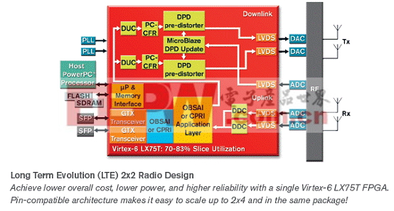
图2. LTE 2x2无线电设计框图(无线基础设备)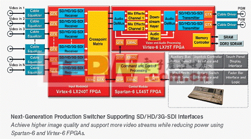
图3.支持SD/HD/3G-SDI接口的新一代交换框图(广播通信)


评论