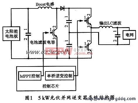
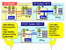
为电网注入绿色能源

虽然能效和行业标准是光伏逆变器技术发展的主要推动力,但可靠性也是一个重要的因素。
现代环保建筑的最新趋势是蓝色 ── 更正确来说应该是深蓝色的太阳能板。即使是经济危机和各国政府降低可再生能源的收购价格,也无阻这个发展势头。
现在,这些太阳能发电系统的拥有者已不在乎太阳能板会不会影响建筑外观,而是关注如何提高系统的发电量和可靠性。(不要忘记,在1990年代,所谓“能效”是指在整个系统寿命期间产生超过7000功率温度周期(power temperature cycle)而已!)
《为电网注入绿色能源》一文 (英文版) 将讨论良好可靠的电源开关如何为绿色电源建立关键的基础。
Photovoltaic systems can be found almost anywhere now. It all started in Germany, today the biggest market for PV systems and home of the biggest cell and inverter manufacturers, and at the same time enjoying a solar irradiation level similar to Alaska. These systems have seen tremendous technological development over the last years, both in panel efficiency as well as inverter technology. While the panel efficiency is driven largely by fundamental research in how to make a photo diode more efficient, the PV inverter is a fine example of power electronics at its best.
The main factors driving development in PV inverters really are efficiency, reliability, and compliance with existing and upcoming regulations, as well as improving the cost. At the same time, new developments in cell technology beyond monocrystalline silicon are forcing changes in the specifications too.
It is easy to see why efficiency matters the more kilowatt-hours the system puts out, the better. Let’s take an example of two 5-kWp systems, with the inverters having 95% and 96% efficiency. With an average working time of 1,200 h/year and an estimated yield of 80%, the input will be equivalent to 4,800 kWh, and at 1% improved efficiency the better system will produce around 50 kWh more, per year. At current feed-in tariffs this amounts to $34/year, or almost $700 over the expected lifetime of the system!
Reliability is also very important, since maintenance cost for remote systems can be quite expensive. This isn’t simply about the repair cost, since when the inverter is not working, no energy is being fed into the grid, so the yield loss also must be considered.
Today, four different panel types dominate the market:
The efficiency values are industry-average estimates for mass production, and as such can only give a relative indication. Today, around 85% of all panels are built with c-Si (see Fig. 1). But the other cell types are quickly catching on, driven by the fact that less raw materials are needed for making them.
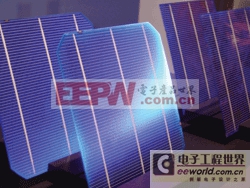
Fig. 1. Monocrystalline silicon cell.
There is a drawback however – the new panel types have a higher ratio of no-load voltage to the voltage at maximum output power, and this implies that the inverter input section must be capable of supporting these higher voltages while at the same time showing good conversion efficiency at lower operating points.
The inverter is the main element between the panels and the grid. It provides proper loading to the cells, to draw the maximum power, and converts this energy into an ac output current.
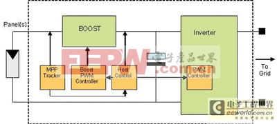
Fig. 2. The maximum power point tracker helps the inverter draw the maximum power for the inverter to convert to ac output current.
To do this, a maximum power point (MPP) tracker (see Fig. 2) is used. The cells can be thought of as a voltage source with a non-linear source impedance, and the MPP tracker varies the loading until the product of voltage and current is maximized, by changing the input impedance of the boost converter.
In a second stage, this dc current is then converted into the required ac output current. For this, the inverter monitors the grid voltage and frequency, and its own output current, to appropriately control the inverter stage.
The inverter really works as an ac current source, driving the grid impedance. The intermediate voltage has to be higher than the desired peak output voltage, plus some margin – at 220 Vrms, the peak voltage is 308 V, so the intermediate dc bus voltage is usually chosen to be 350 to 390 V. This means the second inverter can act as a pure step-down circuit, simplifying the topology.
It is not uncommon to find several boost converters connected in parallel, to be able to connect multiple strings of panels. They all feed into one inverter.

Fig. 2. The maximum power point tracker helps the inverter draw the maximum power for the inverter to convert to ac output current.
Figure 3 shows an inverter, with the main PCB dedicated to the power conversion. In the center, power IGBTs can be seen under clips that press them to a heat sink. On the right, electrolytic caps are used as intermediate caps between the boost converter and the inverter, to store the energy needed to bridge individual 50 Hz cycles. This is a transformer-less inverter, and the two big inductors on the top are the output inductors.
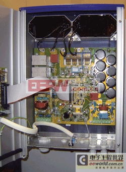
Fig. 3. Small inverter for 3kWp output power.
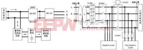
Depending on safety requirements and, to some extent, the panel types and installation, a PV inverter may be required that provides isolation. This can be done with a transformer, where the inverter from above block diagram will drive the transformer with a high frequency, and then a second stage with rectification and dc to ac conversion is required to produce 50 or 60 Hz ac for feeding the grid. Unfortunately, this means the efficiency drops by 1% to 2%.
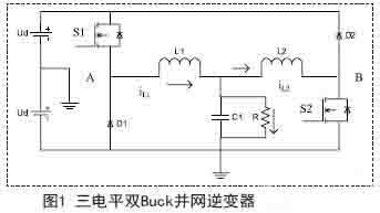
Topology choice
Figure 4 shows the classical topology of a boost converter, followed by a H-bridge. The transistors Q1 and Q2 are parallel, which is not uncommon in this stage and done simply to achieve lowest conduction losses.

Fig. 4. Typical boost converter followed by H-converter bridge.
This stage is followed by a capacitor, to stabilize the voltage that goes into the H-bridge and provide a certain holdup time. This capacitor will have to be an electrolytic capacitor in many cases, due to the size required, and this is probably the most important factor determining system reliability the inverter will see around 7,000 temperature cycles in a 20-year lifetime, and this is a huge strain for electrolytic caps.
In the inverter or dc-to-ac section of the system, some of the devices can be switched at line frequency whereas others are switched with the conversion frequency. If done cleverly, the first devices can be chosen for lowest conduction losses, like the non-punch-through (NPT) Fieldstop (FS) IGBTs from Fairchild Semiconductor, whereas the latter should be chosen for lowest switching losses.
Here, a combination of different IGBTs or even IGBTs and MOSFETs can help to improve the overall yield. And to properly drive the power switches, optically isolated gate drivers like Fairchild’s FOD3180 can be used, improving the system reliability where high dv/dt can suddenly occur, such as in the case of a grid fault.
The topology choice also implies a certain method to adapt the output behavior to the grid load. Here, new regulations are being implemented, forcing the inverters to contribute more to the local grid quality than before.
In certain areas, where many PV systems are connected, the phase lead of the output current of the inverters can lead to local breakdowns, simply due to the interaction between the inverters’ regulation loops. This needs fixing, by imposing certain limits on grid frequency as well as a requirement for the inverters to provide reactive power, that means, the current lagging the voltage.
The choice of best-in-class power switches like Fairchild’s SupreMOS can help to significantly improve efficiency, since in this application, the losses are still largely dominated by what is happening in the power switches. Additionally, further integration of subsystems into intelligent power modules is a candidate to further increase both efficiency and reliability. Due to the close proximity and ideal matching of driver and power switch, the best possible switching behavior can be realized repeatedly.


评论