限制稳压器启动时dV/dt和电容的电路

有时,设计约束突出地暴露了平凡器件和电路的不利方面。这种案例有供电源稳压电路的设计,电路中一次电源有完全限流规定,例如太空船的光电或“日光”板和放射性同位元素热电发生器。这种应用需要谨慎严格的控制电流消耗,包括瞬变电流消耗和罕见消耗尖峰,例如那些上电时典型发生的。问题是限流一次电源即使响应瞬间的过流故障,都会损害灾难性的电压降并关闭。通常这种故障由稳压器输出的去耦电容释放的电流尖峰引起。
除非稳压器限流削弱发生的尖峰,尖峰与稳压器输出电压上升速率与并联输出总电容的乘积相等:IMAX=dV/dt×COUT,其中IMAX是最大电流,dV/dt为电压对时间的微分,COUT为输出电容。公式表明限制稳压器接通最大电流的最佳策略是限制dV/dt。如图1电路基于这个方法,使用工业标准的可调线性稳压器,例如流行的low-dropout LM2941。
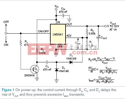
限制dV/dt方法的基础包含6个额外器件:R3、R4、CT、D1、D2和Q1。上电时,控制电流通过R3、CT和D2使输出电压上升延迟,因此阻止了过大的瞬时最大电流。
下面是其工作过程。当VIN打开且Q1关闭时,电流通过R3、CT和D2上拉稳压器参考端到参考电压。这个动作限制了VOUT 的dV/dt到CT通过串联电阻放电的速率,(R3+R1R2/(R1+R2)),使用公式R3=(VIN–VREF–1)/VOUT,R4=20R3,和CT=COUTVOUT/(IMAX(R3+R1R2/(R1+R2))),从而限制IMAX到任何需要值。例如,假定电路如图所示,COUT=100 μF,dV/dt=2500V/s,且IMAX=0.25A。在改进的上电序列后部,D1和D2从稳压器反馈网络中分离dV/dt电路,防止从输入到输出纹波电压的耦合。
英文原文:
Circuit limits dV/dt and capacitor inrush at regulator turn-on
Adding a simple circuit to the adjust pin of a regulator controls the dV/dt of the output voltage, limiting inrush current.
W Stephen Woodward, Chapel Hill, NC; Edited by Charles H Small and Fran Granville -- EDN, 10/11/2007
Unusual design constraints sometimes reveal the unfriendly side of everyday components and circuits. A case in point is the design of power-supply-regulation circuitry in which the primary power source has an absolute current-limit specification, such as spacecraft photovoltaic, or “solar,” panels and radioisotope-thermoelectric generators. Such applications require that you pay scrupulous attention to strict control of current consumption, including transient-current consumption, and infrequent consumption spikes, such as those that typically occur on power-up. The problem is that current-limited primary-power sources can suffer catastrophic voltage droop and shutdown in response to momentary overcurrent faults, even when the fault is brief. Common causes of such faults are the current spikes that charge the regulator output’s decoupling capacitor.
Unless the current limit of the regulator clips the resulting spikes, the spikes are equal to the regulator’s output-voltage rate of rise multiplied by the sum of the parallel output capacitances: IMAX="dV/dt"×COUT, where IMAX is the maximum current, dV/dt is a differential in voltage with respect to a differential in time, and COUT is the output capacitance. The math suggests that the best strategy for limiting the regulator’s turn-on maximum current is to limit dV/dt. The circuit in Figure 1 relies on this trick and works with industry-standard adjustable linear regulators, such as the popular low-dropout LM2941.
The basis of the dV/dt-limiting technique comprises the six added components: R3, R4, CT, D1, D2, and Q1. On power-up, the control current through R3, CT, and D2 delays the rise of the output voltage and thus prevents excessive maximum-current transients.
Here’s how it works. When VIN is on and Q1 is off, current through R3, CT, and D2 pulls the adjust pin of the regulator to the reference. This action limits VOUT’s dV/dt to the rate of CT charging through the series resistance, (R3+R1R2/(R1+R2)), and thereby limits IMAX to any desired value using the design equations R3=(VIN–VREF–1)/VOUT, R4=20 R3, and CT="COUTVOUT/"(IMAX(R3+R1R2/(R1+R2))). For example, given the circuit constants in the figure and assuming COUT="100" μF, dV/dt=2500V/s, and IMAX="0".25A. At the end of the modified power-up sequence, D1 and D2 decouple the dV/dt circuit from the regulator’s feedback network, preventing the coupling of ripple voltages from the input voltage into the output voltage.
英文原文地址:http://www.edn.com/article/CA6486029.html

基尔霍夫电流相关文章:基尔霍夫电流定律
评论