交点分析运算放大器电路-Nodal Analysis of

The Basics
No electronic component is perfect and the op amp is no exception. As usual, we assume an ideal op amp with the understanding that real-world limitations may need to be considered at some point.In particular, we assume infinite input impedance and zero output impedance. The front end of the circuit is not loaded in any way by the op amp and its output can source or sink as much current as needed to faithfully respond to the input. With these assumptions and op amp configurations with negative feedback, the voltage at the two inputs is identical and the output adjusts itself to a voltage to maintain this state.
It is also assumed that the bandwidth of the op amp is sufficient to respond to the needs of the circuit and the open loop gain of the amplifier is infinite.
The performance of modern components is such that in most cases, the above assumptions are perfectly acceptable and very little performance degradation occurs as we move away from the ideal.
Nodal Analysis
Long before the op amp was invented, Kirchoff's law stated that the current flowing into any node of an electrical circuit is equal to the current flowing out of it. (There are conditions on Kirchoff's law that are not relevant here.) An op amp circuit can be broken down into a series of nodes, each of which has a nodal equation. The equations can be combined to form the transfer function.Consider the circuit at the input of an op amp. The current flowing toward the input pin is equal to the current flowing away from the pin (since no current flows into the pin due to its infinite input impedance). The same cannot be said for the output, since the op amp can source or sink current.
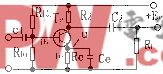
Current-to-Voltage Converter
A simple current-to-voltage converter is shown in Figure 1. Its behavior can be easily understood using the previously explained nodal analysis. The input current (IIN) flowing into the inverting input is equal to the current flowing out of it through the feedback resistor (R). This current creates a potential drop across R, given as:V = IIN × R.
As explained earlier, the voltage at inverting input is equal to that applied at the noninverting input because the circuit has negative feedback; that is, the inverting input is fixed at VREF. This "virtual ground" at the inverting input implies that the op amp continuously adjusts its output voltage (VOUT) to maintain the IIN current flowing through R. VOUT is at VREF with zero input current, and it decreases proportionally for an increasing IIN. The following equation results:
VOUT = VREF - (IIN × R)
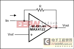
Figure 1.
Differential Amplifier
Taking this notion one stage further, Figure 2 shows a differential amplifier. Its transfer function can be calculated by again considering the currents flowing into and out of the nodes.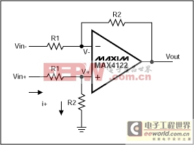
Figure 2.
Consider the current flowing towards the non inverting pin. This can be represented by:
Similarly, current flowing away from that node can be represented by
Combining Equation 1 into Equation 2 gives
Now, life is made easier if we use conductances instead of resistances (it keeps the fractions to a minimum). Thus,
where
so
therefore the voltage V+ is given by
The nodal equations for the inverting node are just as straight forward
To find a transfer function, we know
Combining Equation 3 and Equation 5 into Equation 4 gives
so
In other words, the output depends on the differential voltage across the inputs and the gain-setting resistors, as we would expect.
Wien Bridge Oscillator
The technique of nodal analysis can be used to analyze circuits with reactive components. In the same way we considered the conductances of resistors, with reactive components the equations are made easier by considering their admittances. A capacitor has an admittance of sC. Note that the Laplace nomenclature is used, since again it makes the equations look easier and the psychological effects of this are considerable. We could equally use jw in place of s if we wanted to get an idea of the phase effects of a circuit and this will be done later.Boldly going forth with the above supposition, a Wien bridge oscillator can now be analyzed. Figure 3 shows the generic configuration of this circuit. Again, to keep the equations simple most engineers keep the resistor values equal and the capacitor values equal. In this circuit we have both parallel and series networks, so it makes no difference to the simplicity of the math if admittances or reacta 电流传感器相关文章:电流传感器原理


评论