高侧电流传感器输出周期

High-side current monitoring is found in many battery-powered products that require accurate monitoring of load current, charger current, or both. In non-portable applications high-side current monitoring serves as a power-supply watchdog that can flag a failure in downstream devices. It can also eliminate hazardous conditions by preventing power-supply overloads. Further, high-side current monitoring of motor/servo currents can produce useful feedback in a control application.
What's needed in these applications is a device that converts high-side current directly to a digital signal (Figure 1). IC1 is a low-cost, high-side current-sense amplifier that converts high-side current to a proportional ground-referenced voltage. Its two internal comparators (latching and non-latching) implement a voltage-to-pulse converter that produces a pulse-width output proportional to the measured current.
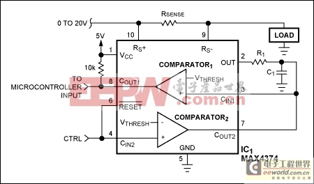
Figure 1. The duration of a negative-going pulse at COUT1 (pin 8) is proportional to the current flowing through Rsense.
IC1's OUT pin charges C1 via R1. When the C1 voltage reaches 0.6V, comparator 1 latches in the high-impedance state. The time required to charge C1 to 0.6V is proportional to the current being measured. Comparator 2 in conjunction with the RESET pin initiates the conversion and removes the pre-charge on C1.
Conversion is controlled by the RESET and CIN2 pins, tied together and connected to a TTL-compatible MCU output (CTRL). Normally, CTRL is high. The MCU starts a conversion by pulsing CTRL low, which discharges C1 and clears the latch on comparator 1 (COUT1 goes low). The MCU now measures time from the CTRL output transition to the low-to-high transition at COUT1 (Figure 2). (The period begins at the low-to-high transition of CTRL and ends at the low-to-high transition of COUT1.)
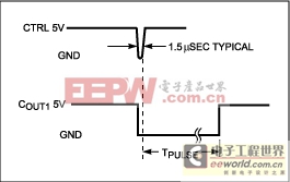
Figure 2. These waveforms illustrate operation of the Figure 1 circuit.
In response to the current levels of interest, RC is selected to create pulse durations in the tens of milliseconds. As a result, the OUT settling time (20µsec) and the comparator propogation delays (4µsec) have negligible effects on the measurement accuracy. To derive an expression for the output pulse width, start with the relationship for an RC-charging circuit:
Vthresh = Out(1 - ε-Tpulse/R1C1)
For "Out" (voltage at the Out terminal in Figure 1), substitute the expression (Iload × Rsense × Av), and solve for Iload:
Iload = Vthresh/(Rsense × Av(1 - ε-Tpulse/R1C1)), where
Iload = measured current in amps
Vthresh = comparator threshold = 0.6V
Rsense = current-sense resistance in Ω
Av = gain of IC1
Tpulse = time required to charge C1 to Vthresh (in seconds)
For example, when selecting R1 = 1M, C1 = 0.1µF, Rsense = 0.075Ω, and Av = 20; this produces a Tpulse measurement of 0.022 seconds in response to a 2A current. Thus, given an MCU timer port, an external interrupt, or simply an available MCU input, IC1 and two external passive components implement high-side current-to-digital conversion without need for a discrete A/D converter.
A similar version of this article appeared in the March 7, 2002 issue of EDN magazine.

基尔霍夫电流相关文章:基尔霍夫电流定律


评论