On Semi Q32M210 32位MCU血糖仪应用方案

On Semi公司的Q32M210是精密的混合信号32位MCU, 集成了2个16位模数转换器、高精度电压参考、3个10位数模转换器和基于ARM® Cortex-M3 32位内核以及高度可配置的模拟前端及可编程的32位内核和256kB闪存.芯片还集成所有关键功能,包括实时时钟、电源管理、112段液晶显示屏(LCD)接口、片上低阻抗开关、非限定(uncommitted)运算放大器、精密电压参考( 50 PPM/℃)及电阻电容(RC)振荡器。器件具有高精度感测,可预测工作以及低功耗等特性,主要用于便携感测应用如病人监测器、无线心电图机(ECG)和血糖仪等便携医疗设备.本文介绍了Q32M210主要特性,方框图, 正常工作条件配置图以及典型和扩展电源配置图, 血糖仪应用电路图和相应的材料清单.
Q32M210 is a precision, mixed−signal 32−bit microcontroller. Themicrocontroller is built on the high performance ARMCortex_−M3 processor.
The microcontroller incorporates a highly configurable sensor interface designed to work directly with a wide range of sensors having multiple characteristics, including specialized electrochemical sensors. The sensor interface includes dual programmable gain amplifiers, dual 16−bit Analog−to−Digital converters, triple 10−bit Digital−to−Analog converters (for voltage waveform generation and other applications) and three uncommitted, low−noise opamps with configurable signal multiplexing. Flexible connectivity to external non−volatile memory, personal computers, wireless devices, LCD displays and a wide range of other peripherals is enabled by several digital interfaces including I2C, USB (2.0 full−speed compliant) and a high−speed SPI/SQI interface.
The microcontroller features flexible clocking options as well as intelligent failure monitoring of power and application interruptions required by high performance, portable, battery operated applications.
All necessary clocks including an internal oscillator, real−time clock and a dedicated clock for USB operation are available on−chip (external crystals required for RTC and USB).An embedded power management unit, which incorporates several low power modes, allows application developers to minimize both standby and active power under a wide range of operating conditions.
The ultra−low sleep current makes the microcontroller ideal for applications that remain inactive for long periods of time. A large on−chip non−volatile flash memory (256 kB) combined with on−chip SRAM (48 kB) supports complex applications and simplifies application development. The flash contains built−in hardware error checking and correction (ECC) for application reliability. Additionally, a configurable DMA unit which supports independent peripheral−to−memory, memory−to−memory, and memory−to− peripheral channels provides flexible, low power data transfers without processor intervention.
A suite of industry−standard development tools, hands−on training and full technical support are available to reduce design cycle time and speed time−to−market.
Q32M210 主要特性:
Ultra Low−Power and Smart Power Management
Less than 400 _A / MHz, up to 16 MHz clock speed
Reliable operation down to 1.8 V; 3.3 V nominal supply voltage
Ultra−low−current sleep mode with Real−time Clock active ( 750 nA)
Low−current standby mode with register and SRAM retention ( 26 _A)
Integrated power supplies minimize need for external components. Only a minimum of external passives is required
Efficient, Powerful and Robust Processing Architecture
32−bit ARM Cortex−M3 CPU
256 kB on−chip flash with integrated hardware ECC for program and user data storage
48 kB on−chip SRAM
Flexible DMA, 4 general−purpose timers, CRC calculator
No external voltage required for flash write operation
Low−Noise, Low−Leakage, Low−Temperature Drift, Configurable Sensor Interface
Triple ultra low−noise opamps with low−leakage inputs and configurable outputs
Dual on−chip Programmable Gain Amplifiers (PGA) and ADCs with flexible input multiplexing and wide dynamic range
Reconfigurable voltage detection unit
Optimal dynamic range scaling of sensor signals
Flexible on−chip signal routing for dynamic reconfigurability
Minimal temperature drift of gain and offset errors allows for precise calibration
Built−in Temperature Sensor
Predictable Operation
Dedicated brown−out protection circuit prevents execution of code outside of operating range
Integrated hardware−based ECC for on−chip flash maintains code and data integrity
Watchdog timer
High Precision Analog−to−Digital Conversion and Digital−to−Analog Conversion
Dual 16−bit ADCs with on−the−fly data rate configurability
Triple 10−bit DACs with configurable dynamic range
Precision Voltage Reference
On−chip, low temperature drift ( 50 ppm/C) voltage reference for ADCs and DACs
Flexible On−Chip Clocking
Processor supports speeds up to 16 MHz provided either through internal oscillator or externally supplied clock
Flexible Sensor Interconnections
Triple low Ron analog multiplexers, including an 8:1 input mux
Quad SPST and quad multi−switches for effective simultaneous connection to different sensors
USB 2.0 Full−Speed Interface
Built−in transceiver for 2.0 Full−speed compatible (12 Mbps) operation with dedicated power supply
Flexible External Interfaes
Configurable Interface Wakeup pins with configurable pull−ups and pull−downs
8 Configurable GPIO interrupts
Dual UARTs, dual SPI, SQI, I2C, PCM (including I2S mode), GPIOs
LCD Interface
Up to 112 segments with integrated charge pump and backlight driver (up to 10 mA)
Packaging
Available in 140−pin TLLGA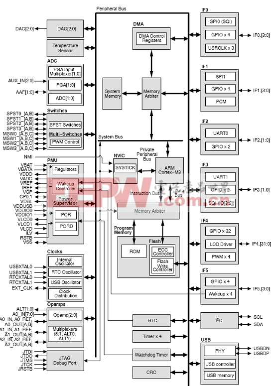
图1. Q32M210功能方框图
图2. Q32M210正常工作条件配置图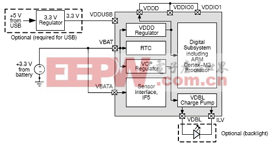
图3. Q32M210典型电源配置图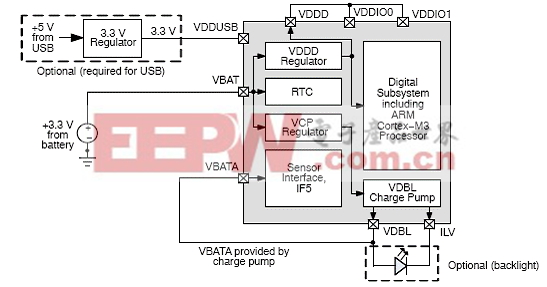
图4. Q32M210扩展的电源配置图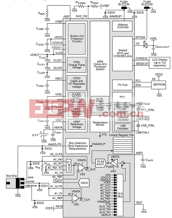
图5. Q32M210血糖仪应用电路图
血糖仪应用材料清单: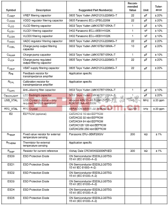
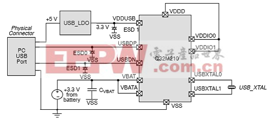
图6. Q32M210 USB应用电路图
USB应用电路材料清单: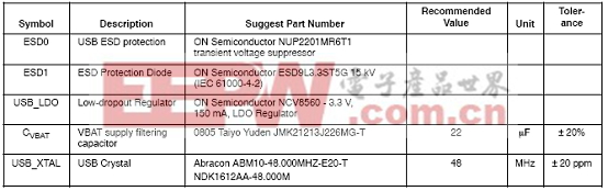


评论