具有电绝缘、线或能力和改进噪声限的I2C接口设计

本设计方案讲解了一个简单而又有效,为连接在I2C总线上的设备提供光绝缘体的方法(如图1)。这个电路改进了参考文献1的早期版本。SDA和SCL是I²C总线的主区域;SDA1和SCL1是I²C总线的从区域。由于时钟线是无方向性的,相当容易实现主从设备间的光绝缘。P沟道MOSFET Q3提供隔离时钟线的高速光耦IC2中的发光二极管电流。
本文引用地址:https://www.eepw.com.cn/article/78553.htm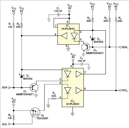
图1 电路提供由从设备到I2C总线主设备的绝缘、双向、线或连接
但数据线是双向的,且这部分电路是对称的。电阻R6和R7是I²C总线从设备边的上拉电阻,而R3和R1为虚上拉电
阻,位于SDA/SCL一边且平行于主I²C上拉电阻。如果SDA和SDA1线都为高——也就是说,没有I²C设备使其为低——Q1将截止,没有电流流进光耦IC2的发光二极管,IC2管脚7为高,Q2截止,并且光耦IC1的发光二极管也截止。
如果有设备驱动SDA线置低,IC2的发光二极管关闭,驱动IC2的7管脚为低;然后二极管D2开始导通。结果SDA1线处于低状态——IC2的低输出电压加上肖特基二极管D2的阈值电压。在这种情况,注意到IC1的发光二极管没有打开是重要的,因为它两端电压低于阈值。这意味着电路没有锁存,一旦SDA线被释放,它将恢复。
Q3、PNP BJT(双载子接面电晶体)和Q1有效的缓冲SDA/SCL两条线,所以当连接总线的开集和开漏部分I²C设备的线持续为低时,没有额外的电流流进。这个机构允许电绝缘接口重复拉低提供线或能力。使用肖特基二极管D1和D2,而不是普通二极管,为的是减少总线上低状态电压,改进噪声极限。最后,由于本设计使用Fairchild半导体HCPL06XX设备具有低传播延时的特征,接口没有总线脉冲干扰问题,并且能够以400 kHz或更高的速度工作。
英文原文:
I²C interface has galvanic isolation, wired-OR capability, improved noise margin
You can use optoisolators to galvanically isolate the slave devices on an I2C bus from the master device.
Michele Costantino, Microsaic Systems Ltd, Woking, United Kingdom; Edited by Charles H Small and Fran Granville -- EDN, 7/5/2007
This Design Idea describes a simple and effective way to provide optoisolation for devices connected on the I²C bus (Figure 1). It improves on an earlier version (Reference 1). SDA and SCL are on the bus master’s side of the I²C bus; SDA1 and SCL1 are on the slave device’s side. It is fairly easy to optoisolate the clock line because it is unidirectional, from the master to the slave device. A P-channel MOSFET, Q3, provides the current for the LED of the fast optocoupler, IC2, buffering the clock line.
The data line, however, is bidirectional. This section of the circuit is symmetrical. Resistors R6 and R7 are the I²C pullup resistors on the slave device’s side of the bus, and R3 and R1 are dummy pullups in parallel with the main I²C pullup resistors on the SDA/SCL side. If both SDA and SDA1 lines are high—that is, no I²C devices are pulling them down—Q1 is off, no current flows into the LED of optocoupler IC2, IC2’s Pin 7 is high, Q2 is off, and the LED of optocoupler IC1 is also off.
If a device drives the SDA line low, Q1 and the LED of IC2 turn off, driving IC2’s Pin 7 low; diode D2 then starts to conduct. The result is a low level on the SDA1 line—the low output voltage of IC2 plus the threshold voltage of Schottky barrier diode D2. In this situation, it is important to notice
that the LED of IC1 does not turn on because the voltage applied across it is below its threshold. This situation means that the circuit does not latch, and it can recover from this state once you release the SDA line.
Q3 and the PNP BJT (bipolar-junction transistor), Q1, effectively buffer the two SDA/SCL lines so that no extra current flows into the open-collector and -drain stages of the I²C devices that connect to the bus when they hold the lines down. This configuration allows the optoisolated interface to repeatedly pull low, providing wired-OR capability. Using Schottky barrier diodes for D1 and D2 rather than common diodes reduces the low-level voltage on the bus, improving the noise margin. Finally, because of the low propagation-delay times of the Fairchild Semiconductor HCPL06XX devices that this design uses, this interface has no bus-glitch problems and works well at speeds of 400 kHz or higher (Reference 2).
References
Nguyen, Minh-Tam, and Martin Baumbach, “Two-wire interface has galvanic isolation,” EDN, Nov 11, 1999, pg 174.
Blozis, Steve, “Opto-electrical isolation of the I2C-Bus,” Embedded Systems Design, Oct 14, 2004.

评论