LED背光boost驱动器

Abstract: This is a reference design for an LED display-backlight driver. The design uses a boost power supply with adaptive feedback for efficiency and linear current sinks for a high dimming ratio (2000:1). The input voltage is 8V to 18V with 50V transients, and the load is three parallel strings of 8 LEDs (34V) at 150mA/string. TheMAX1680916-channel LED driver is featured.
This reference design is an LED backlight driver for a TFT display. The electrical input requirements and output capabilities follow:
VIN: 8VDC (at 1.667A) to 18VDC (at 730mA); tolerant to 50VDC transients
PWMIN: 250Hz pulse train; 2µs (min) pulse; > 3.3VDC at 0mA; 0.3VDC at 10mA
VLED config.: 6 or 8 LEDs (2.89VDC to 4.2VDC) in series (34VDC max); three parallel strings, 150mA per string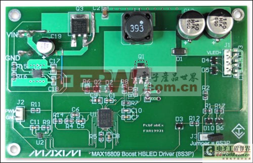
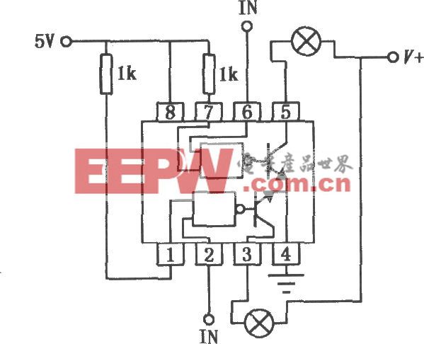
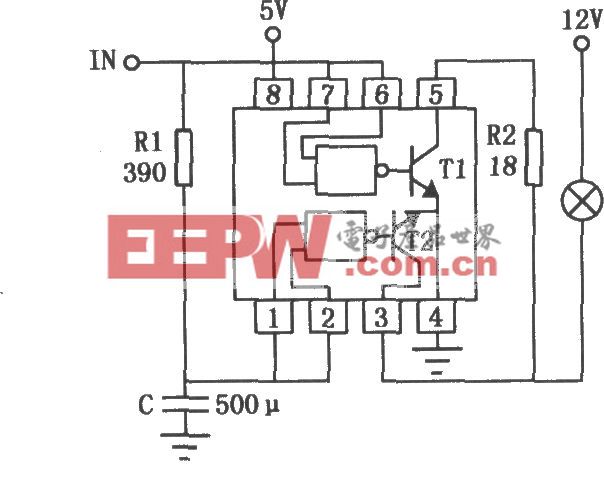
Figure 1. The driver board features the MAX16809.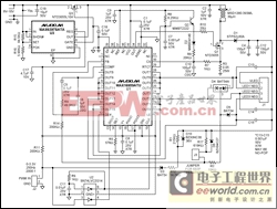
More detailed image (PDF, 6.61kB)
Figure 2. Schematic of the driver design.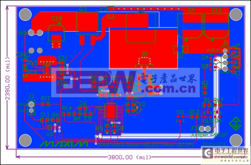
Figure 3. Layout of the driver design.
Brief Circuit Description
This reference design uses the MAX16809 as a central controller for a boost power supply and a 16-port LED driver. Fifteen of the sixteen ports are grouped into units of five to drive three parallel strings of LEDs. With boost power supplies the output voltage is always greater than the input power-supply voltage. The boost power supply operates at a frequency of 200kHz, which is fast enough for small power components and yet slow enough to prevent overheating the switching MOSFET.
The design uses two low-ESR, electrolytic capacitors on the output. These capacitors are necessary to absorb the inductive energy of the power supply when the PWM signal shuts the load to zero. The output voltage for the LED strings is available through a 4-pin header. VLED+ is pin 1 of the header, while pins 2, 3, and 4 are the VLED- pins. Pads for output filter capacitors are available if desired; they are presently not populated. The Q2-D2-R8 circuit provides slope compensation for the current-mode PWM controller. This circuit, which follows the RTCT ramp voltage, injects current into R7and thus creates a ramp voltage that helps prevent subharmonic oscillation of the controller at duty cycles greater than 50% (when the input voltage is at the lower end).
The boost feedback path has two modes: adaptive and resting. The adaptive mode (when the PWM signal is high) will "diode-OR" the outputs so that the lowest driver voltage (largest series LED string voltage) is regulated to about 1.0VDC. This provides enough headroom for proper operation of the LED driver. Other LEDs strings will have a lower series voltage, and thus the drivers will have greater headroom. Adaptive mode minimizes the power dissipation caused by the linear LED drivers. For this approach to work, although the absolute LED voltage drop is not critical, the relative forward voltages must be matched to within 200mV of each other. To dissipate the heat, the MAX16809 must have a good thermal connection to large copper planes using thermal vias beneath the exposed pad of the package. On this board, the bottom plane provides cooling to the IC, but multiplane grounds with larger surface areas will dissipate the heat even better.
In the resting mode (when the PWM signal is low), VLED is regulated like a conventional power supply; the voltage rises to a value that will guarantee operation for very short pulses. Since the power-supply magnetics cannot charge quickly enough for short pulses, all of the energy must originate from the output capacitors. The resting mode ensures that the capacitors are charged enough to sustain this energy until the magnetics can respond. Ironically, the input current may surge more at the beginning of the resting mode than during the adaptive mode. This happens because the large output capacitors need to be charged. For much of the on-time, the adaptive energy comes solely from the output capacitors, the switcher rests, and the input current drops to zero.
Zener diode, D10, provides overvoltage protection to the circuit. If an LED string becomes disconnected, the adaptive voltage control would attempt to increase VLED to satisfy the 1.0VDC requirement. D10 limits the output voltage to 38.5VDC. While this voltage will not harm the circuit, the resulting power dissipation in the LED drivers will overheat the MAX16809. If this occurs, the chip's internal circuitry will power the drivers down until the temperature is reduced. The resulting effect is LED blinking. For 6S3P operation, install a jumper on connector, J3, which will place D6 in parallel with D10 and lower the clamp voltage to 29VDC.
The LED drivers are set to 30mA through R5 (576Ω). By paralleling five drivers per LED string, the IC provides 150mA per string.
A Schmitt-triggered inverter, U2, is configured as an oscillator to provide a clock to the SPI™ input of the MAX16809. Since DIN is connected high, a string of "1s" is clocked into internal registers which enables all the LED drivers. U2 also inverts the PWM signal to meet the requirements of the MAX16809 OE# input.
U3 (aMAX6397TATA overvoltage protection circuit) provides input protection to the circuit during a load dump, and provides a 3.3VDC power supply for the linear drivers in the MAX16809. R15/R16 set the shutdown voltage to a nominal voltage of 18.85VDC. Q3 is sized for minimal drop at low-input voltages. At full load, the nominal minimum operating voltage was measured at 7.82VDC. The REG output supplies 3.3VDC to the MAX16809's linear drivers (V+ input), to U2, and to the R11 pullup resistor.
Test and Performance Results
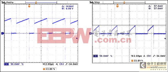
Figure 4. MOSFET current and voltages with VIN = 18V and with VIN = 36V.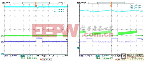
Figure 5. VLED and input current with 1µs pulse and with a 1ms pulse. VLED alternates between resting mode and adaptive mode. Note that the input current surges to provide a charge to the output capacitor during the resting mode.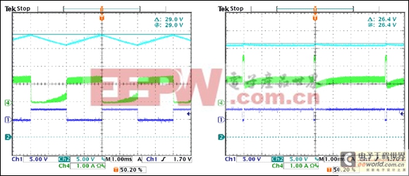
Figure 6. VLED and input current with a 2ms pulse and with a 3.9ms pulse.
Temperature Measurements
The following temperatures were measured using loads provided by OSRAM:
| VIN | 8VDC |
| Ambient | +20°C |
| TU1 | +38°C |
| TU3 | +36°C |
| TQ1 | +37°C |
| TQ3 | +34°C |
| TL1 | +37°C |
| TD1 | +37°C |
| VIN | 36VDC |
| Ambient | +20°C |
| TU1 | +39°C |
| TU3 | +45°C |
| TQ1 | +32°C |
| TQ3 | +31°C |
| TL1 | +31°C |
| TD1 | +39°C |
Power-Up Procedure
- Attach three strings of 8 LEDs to output connector J1. Alternatively, you can attach three strings of 6 LEDs, if there is a jumper on connector J3.
- The positive side of the LED strings must be attached to pin1 of J1; the negative side of the three LED strings must be attached to pins 2, 3. and 4 of J1.
- Attach an unpowered 8V to 20V (4A rating) to the input wire loops. Be sure to match the correct polarity.
- Turn on the power to the circuit.
- Apply a 250Hz pulse wave to J4. The pulse wave must vary from 0V to 3.3V; the duty cycle can go from 0.05% to 100%.
- Large vias on either side of the current sense resistor, R3, allow for low-noise probing using a ground coil and a single-ended scope probe.


评论