Surge Testing Solid-State USB

Introduction
With a 1.2A current limit one would think that a circuit-protection IC could maintain complete control in the event of a fault or short. The reality is that the current limit usually demonstrates a delay time before the actual shutoff occurs. During a hard short, the current can rise very rapidly, first hitting the DC limit and starting to turn the switch off. (The DC limit is typically an accurate, but slow threshold. A slow threshold avoids nuisance trips from inrush and other spurious events.) A short time later the switch opens, but not before reaching a peak current that can be much higher than the DC limit. Low-inductance leads can cause the current to rise even faster. See Figure 1.Limiting Current by Resistance
Using a MAX1558 USB switch with low inductance leads and a hard short, the current is resistively limited by the internal protection switch. When the protection circuit finally opens, the peak current (I) can be measured. This process is shown in Figure 2. With peak current flowing through the stray input inductance (LSTRAY), energy (E) is stored:E = ½ × LSTRAY × I²
Where does this energy go once the circuit breaker or protection switch finally opens the circuit?
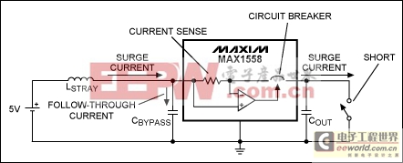
Figure 1. This diagram shows the current path during a hard short and the path for the follow-through current that is driven by stray inductance.
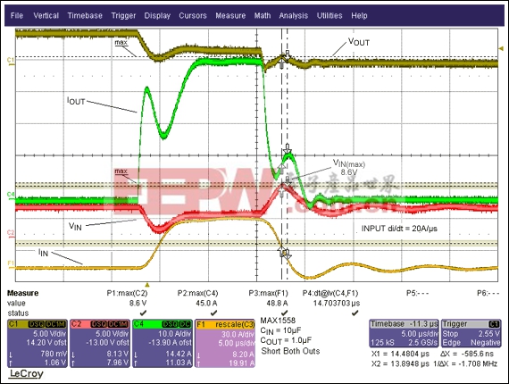
Figure 2. This plot shows the short-circuit performance with a 10µF for CBYPASS. The VIN trace shows that the input soars to 8.6V due to follow-through current.
Looking at Figure 2 we see that the input current (IIN) rises very rapidly to 48.8A, then limits due to resistance. When the switch turns off, we can measure the rate at which the current slews down. With Iin slewing down at 20A/µs and VIN soaring to 8.6V (VMAX), we empirically compute the circuit inductance to be:
(VMAX - VIN) = di/dt × LSTRAY
With VMAX - VIN = 3.6V, and di/dt = 20A/µs, LSTRAY = 180nH.
So with E = ½ × LSTRAY × I², at the end of a fault there is 214µJ stored in LSTRAY. Bypass capacitance is needed to absorb this energy and limit voltage rise. A 10µF input cap with an initial charge of 5V has some initial energy stored:
½ × C × V² = E
Now, assuming that all of the stored energy in LSTRAY will end up in the input cap CBYPASS, then;
Initial Energy + Stray Energy = Final Energy
125µJ + 214µJ = 339µJ
339µJ is then the final energy in the input capacitor, with:
½ × C × V² = E
or
½ × 10µF × V² = 339µJ
Solving for V, V = 8.23V. This closely agrees with the measured value of 8.6V in Figure 2.
Now, if the input bypass is reduced to only 0.1µF, the input voltage can rise up to destructive voltages. So, this time with:
Initial Energy + Stray Energy = Final Energy
1.25µJ + 214µJ = 215µJ
and
½ × 0.1µF × V² = 215µJ
Solving for V, V = 65.6V!
This process, of course, will damage a part rated for 5.5V. The waveforms during this hard short are shown in Figure 3. Notice that the output also soars to 9.8V. This occurred because the short was removed before the switch turned off, which also accounts for the high di/dt in this test. Normally the di/dt is governed by the turn-off characteristics of the power device. With a USB port, the circuit is dependent on the end user—a situation that is anything but controlled. An extremely fast turn-off like this could be caused by an intermittent cable, bad connector, or, as in this case, connection bounce associated with a mechanical connection.
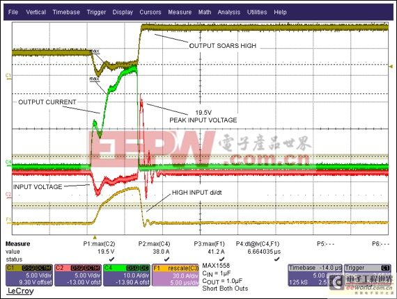
Figure 3. This data shows that with only 0.1µF cap on the input, the input voltage can soar to destructive potential.
Clearly the voltage does not rise to 66V. This is because the part has zenered, thereby clamping the voltage rise and likely suffering damage from the absorbed energy. During such an overvoltage event, the excess energy is absorbed by the silicon chip. A faster closeup of Figure 3 is shown in Figure 4 below.
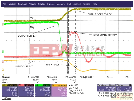
Figure 4. This is a zoom of Figure 3. Notice the high di/dt during turn-off and that some of the stored energy has reached the output! This event destroyed the USB switch.
Figure 4 shows that, with the same circuit, a larger input bypass capacitor provides extra protection from the stray energy that follows a hard short. Normally a printed circuit board (PCB) with a ground plane will have much less stray inductance than the test leads used in this test or that found in a laboratory. When testing in the lab, it is especially difficult to reduce the strays from test leads and test equipment.
Input Inductance Limits Peak Current
Figure 5 shows that even with as much as 1.3µH of input lead inductance, the part can survive with a 10µF bypass capacitor.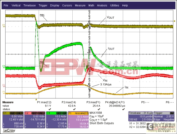
Figure 5. This plot shows the performance with long leads (1.3µH) on the input, but also with a 10µF input bypass. Notice how slow the input current ramps up and down. The part is also zenering so current is spilling over to the output (seen in the IOUT waveform) when the input voltage exceeds 8V, but the switch survives.
Figure 5 shows that the input current slowly ramps up and down due to the larger inductance. This is an important note, indicating that while there is considerably more inductance, the current cannot change as fast. Since energy stored in the inductor is the square of the current and only a linear scale of inductance, high peak currents carry far more energy. The energy stored in the 1.3µH inductor is only 419µJ:
125µJ + 419µJ = 544µJ
and
½ × 10µF × V² = 544µJ
Solving for V as above, V = 10.43V.
While the part did survive this hard short, a larger bypass capacitor is advised and should limit the maximum voltage to under the absolute maximum specified in the data sheet.
Conclusion
Without accounting for the stored energy in stray inductance, USB devices can be subject to overvoltage and even destroyed. Figure 5 shows that input inductance is the limiting factor for peak current, but Figure 2 shows that resistance is the limiting factor. One could conclude that the lower input inductance might perform better. Yet if the current is not limited, the energy for a low-inductance situation can also reach damaging levels. Consequently, care must be exercised to ensure that this does not happen. Figure 2 shows that the current is limited by a resistance of 0.1Ω. Although with reduced inductance the current will ramp up faster, if a current limit is reached, a smaller inductance will store less energy.In most PCB applications, with a ground plane under the protection switch and the input and output traces, the inductance should be much lower than 180nH. A 1/16-inch-wide PCB trace over a ground plane will have approximately 10nH per inch. Each application will have its own circumstances which dictate the size of input bypass that must be deployed. Measurement and analysis of the expected inductance might indicate that a larger bypass is needed to provide reliability. Conversely, it might indicate that a reduced input bypass capacitor is allowed.


评论