选择合适的系列电压基准源的绝对精度电压输出

When designing a system that includes a digital-to-analogconverter (DAC) and an external voltage reference, the voltage-referencespecifications are as important as the specifications of the DAC itself.This article explores some of the issues involved with selecting external,three-terminal series voltage references for voltage-output DACs. Examplesof DAC system designs are used to illustrate the various trade-offs whenoptimizing for cost, accuracy, or power.
A Few Words about Voltage References
The main focus of this article is Maxim's three-terminal, series, bandgap voltage references, although buried-zener references are discussed as well. Two-terminal, shunt references are not covered, because three-terminal, series devices are now available at competitive prices and with low quiescent current that is virtually constant versus input voltage.The MAX6006-MAX6009 two-terminal shunt-reference family is worth considering for ultra-low-power applications, as they can generate 1.25V, 2.048V, 2.5V, or 3V with an operating current of only 1µA. Maxim also offers a family of low-cost, industry-standard LM4040 shunt references.
Zener-based references receive light treatment primarily because of their high input-voltage requirement (which limits their applicability in systems with lower supply voltages). In spite of this narrowing of focus, many topics covered in this article are applicable to other reference types. For example, the reference-voltage change on a shunt reference caused by varying bias currents is analogous to the load regulation of a series reference, and the effect on the DAC performance can be analyzed in a similar manner.
Figure 1 depicts the connection between a three-terminal, series voltage reference (the MAX6325) and a DAC (the MAX5170) for a typical design. In this case, an external capacitor is shown between the reference and the DAC, but it can usually be eliminated if space is limited and if the DAC does not have rapid power supply or output transient switching. The figure also shows a power-supply filtering input capacitor and a broadband noise-reduction capacitor, but both of these capacitors are also optional. Finally, the MAX6325 voltage reference has a TRIM pin that allows the end user to optionally trim out the initial error with an external potentiometer.
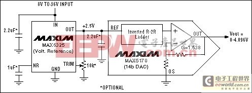
Figure 1. Interfacing a three-terminal series voltage reference and a DAC.
Definitions of Voltage-Reference Specifications
In addition to cost and packaging, several (but not all) specifications will be covered in the discussions on voltage-reference selection. These specifications are described in detail in the references listed at the end of the article, so they will be only briefly summarized here. What follow are definitions of the specifications:Input Supply Voltage: Power-supply input voltage to the reference. Limited on the upper end by the silicon process used for the reference and on the bottom end by the reference output and dropout voltages:
VIN(MIN) = VREF + VDROPOUTReference Output Voltage: Regulated voltage used at the DAC reference input.
Initial Accuracy: Accuracy is a slight misnomer, as it actually represents the initial output-voltage error. Specified in % or mV at 25°C. Some fixed-voltage and any adjustable references can be trimmed to improve accuracy.
Reference Output Current: The available load current that the voltage reference can source to the DAC reference input. All of the references covered in this article can also sink current, but not as well.
Reference-Load Regulation: Incremental change in reference output voltage for a DC change in reference output current. Specified in µV/µA or equivalently mV/mA, mV (over the entire output-current range), ppm/mA, or %/mA.
Input-Line Regulation: Incremental change in reference output voltage for a DC change in input supply voltage. Specified in µV/V.
Output-Voltage Temperature Coefficient (Tempco): Change in reference output voltage for a given change in temperature. Specified in ppm/°C. Maxim uses the box method, where the maximum reference output fractional voltage change is divided by the maximum operating-temperature range:
TCVOUT = 106 ×| ΔVREF(max)/ VREF | / (TMAX-TMIN)Output-Voltage Temperature Hysteresis: Change in reference output voltage at +25°C after a temperature cycle (TMIN to TMAX) is applied. Specified as a ratio of voltages expressed in ppm.
TEMPHYST = 106 × | ΔVREF / VREF |, where ΔVREF = VREF before ΔT cycle minus VREF after ΔT cycle.Output-Voltage Long-Term Stability: Change in reference output voltage versus time. Specified in ppm/1000 hours. Cumulative drift beyond a 1000-hour interval is not specified, but it is usually much lower than the initial drift, which can itself be improved by PCB-level burn-in.
Output Noise Voltage: Voltage noise at the reference output. The 1/f component is specified in µVp-p over a 0.1Hz to 10Hz bandwidth, and the wideband noise is usually specified in µVRMS over a 10Hz to 10kHz bandwidth.
Capacitive-Load Stability Range: Range of capacitive loads (includes user-supplied capacitors, the capacitance presented by the load, and stray capacitance) that the reference can tolerate at its output. External capacitors are needed only to limit large loads or supply transients, and can be eliminated in many designs to save board space. A few references have pins where a compensation capacitor (the MAX872) or a noise-reduction capacitor (the MAX6325) can be added to improve performance.
DAC Considerations
Only buffered-voltage-output DACs are discussed, as the key points are easier to illustrate with this architecture. Current-output DACs are typically used in a multiplying configuration (MDAC) to provide variable gain, and they usually require external op amps to generate a voltage output.All of the Maxim voltage-output DACs considered in this article use an inverted R-2R architecture. From the reference-voltage standpoint, the main characteristic of this DAC architecture is the varying DAC reference input resistance versus DAC code. Care must be taken to ensure that the voltage reference can source enough current at the DAC's minimum reference input resistance and has sufficient load regulation as the DAC codes change. A 4-bit example, along with its normalized reference input current, is shown in Figure 2. Note that the reference current at DAC code 0 is not shown in the plot, as all of the switches connected to the reference are open and virtually no reference current flows. Two other DAC specifications important to voltage-reference selection are reference-input-voltage range and DAC output gain.
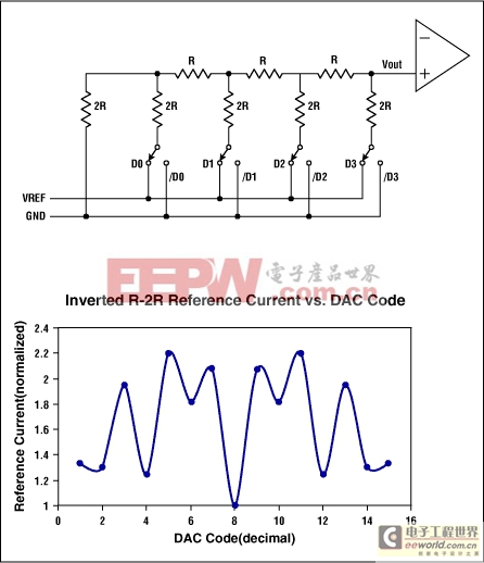
Figure 2. Inverted R-2R architecture and reference-input-current variation (4-bit).


评论