ADI低成本无线ECG Holter监视器解决方案

美国模拟器件(ADI)公司的低成本无线ECG Holter监视器解决方案主要采用12位精密模拟微控制器ADuC7022, 高性能ISM频段FSK/ASK收发器 ADF7022, 低成本仪表放大器AD623, 微功耗精密CMOS运算放大器AD8500和低功耗JFET放大器AD8641等器件.本文介绍了典型的单通道心电图方框图, 低功耗低成本无线ECG Holter 监视器方框图以及主要器件的主要特性和应用电路.
本文引用地址:https://www.eepw.com.cn/article/199385.htmThe ECG signal is characterized by six peaks and valleys labeled with successive letters of the alphabet P, Q, R, S, T, and U.
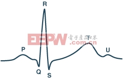
图1.心电图(ECG)的信号波形
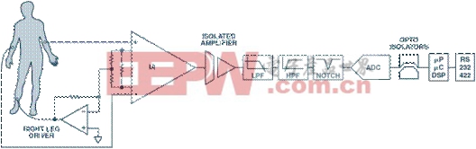
图2. 典型的单通道心电图方框图
Awireless Holter monitor–small enough to fit on the back side of an electrode–provides more accurate signals than traditional designs because noise and interference are greatly reduced. The circuit is inexpensive and capable of providing diagnostic-quality 1-lead ECG traces. A driven leg eliminates the need for a 60 Hz notch filter. Depending on the frequency band used, the transceiver (the ADF702x is shown below) and its surrounding circuitry will change. Patient comfort and privacy is greatly improved because all circuitry can be worn under clothing.
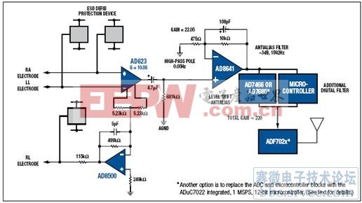
图3.低功耗低成本无线ECG Holter 监视器方框图(1)
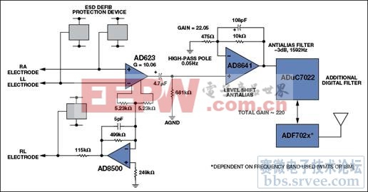
图4.低功耗低成本无线ECG Holter 监视器方框图(2):ADuC7022替代AD7466+MCU
主要元件性能介绍:
ADUC7022: Precision Analog Microcontroller, 12-Bit Analog I/O, ARM7TDMI® MCU
The ADuC7019/20/21/22/24/25/26/27/28 are fully integrated, 1 MSPS, 12-bit data acquisition systems incorporating high performance multichannel ADCs, 16-bit/32-bit MCUs, and Flash/EE memory on a single chip.
The ADC consists of up to 12 single-ended inputs. An additional four inputs are available but are multiplexed with the four DAC output pins. The four DAC outputs are only available on certain models (ADuC7020 and ADuC7026). However, in many cases where the DAC outputs are not present, these pins can still be used as additional ADC inputs, giving a maximum of 16 ADC input channels. The ADC can operate in single-ended or differential input modes. The ADC input voltage is 0 V to VREF. A low drift band gap reference, temperature sensor, and voltage comparator complete the ADC peripheral set.
Depending on the part model, up to four buffered voltage output DACs are available on-chip. The DAC output range is programmable to one of three voltage ranges.
The devices operate from an on-chip oscillator and a PLL generating an internal high frequency clock of 41.78 MHz. This clock is routed through a programmable clock divider from which the MCU core clock operating frequency is generated. The microcontroller core is an ARM7TDMI, 16-bit/32-bit RISC machine, which offers up to 41 MIPS peak performance. Eight kilobytes of SRAM and 62 kilobytes of nonvolatile Flash/EE memory are provided on-chip. The ARM7TDMI core views all memory and registers as a single linear array.
ADuC7022应用:
Industrial control and automation systems
Smart sensors, precision instrumentation
Base station systems, optical networking
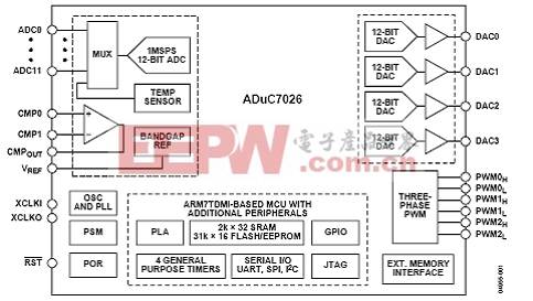
图5.ADuC7026功能方框图
http://www.analog.com/static/imported-files/data_sheets/ADUC7019_7020_7021_7022_7024_7025_7026_7027_7028.pdf
High Performance, ISM Band, FSK/ASK Transceiver IC ADF7020
The ADF7020 is a low power, highly integrated FSK/ASK/OOK transceiver designed for operation in the license-free ISM bands at 433 MHz, 868 MHz, and 915 MHz, as well as the proposed Japanese RFID band at 950 MHz. A Gaussian data filter option is available to allow either GFSK or G-ASK modulation, which provides a more spectrally efficient modulation. In addition to these modulation options, the ADF7020 can also be used to perform both MSK and GMSK modulation, where MSK is a special case of FSK with a modulation index of 0.5. The modula-tion index is calculated as twice the deviation divided by the data rate. MSK is spectrally equivalent to O-QPSK modulation with half-sinusoidal Tx baseband shaping, so the ADF7020 can also support this modulation option by setting up the device in MSK mode.
ADF7020主要特性:
Low power, low IF transceiver
Frequency bands
431 MHz to 478 MHz
862 MHz to 956 MHz
Data rates supported
0.15 kbps to 200 kbps, FSK
0.15 kbps to 64 kbps, ASK
2.3 V to 3.6 V power supply
Programmable output power
−16 dBm to +13 dBm in 0.3 dBm steps
Receiver sensitivity
−119 dBm at 1 kbps, FSK
−112 dBm at 9.6 kbps, FSK
−106.5 dBm at 9.6 kbps, ASK
Low power consumption
19 mA in receive mode
26.8 mA in transmit mode (10 dBm output)
−3 dBm IIP3 in high linearity mode
On-chip VCO and fractional-N PLL
On-chip 7-bit ADC and temperature sensor
Fully automatic frequency control loop (AFC) compensates for ±25 ppm crystal at 862 MHz to 956 MHz or±50 ppm at 431 MHz to 478 MHz
Digital RSSI
Integrated Tx/Rx switch
Leakage current of 1 μA in power-down mode
ADF7020应用:
Low cost wireless data transfer
Remote control/security systems
Wireless metering
Keyless entry
Home automation
Process and building control
Wireless voice
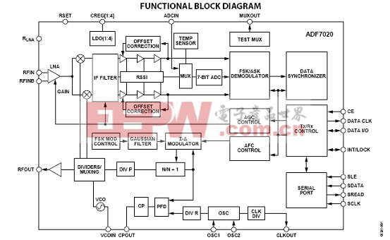
图6. ADF7020方框图
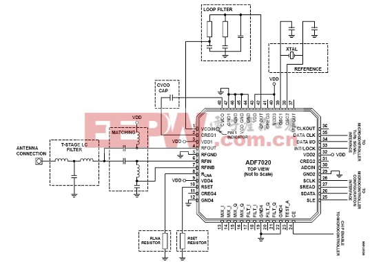
图7.ADF7020应用电路
http://www.analog.com/static/imported-files/data_sheets/ADF7020.pdf
AD623: Single Supply, Rail-Rail, Low Cost Instrumentation Amplifier
The AD623 is an integrated single-supply instrumentation amplifier that delivers rail-to-rail output swing on a 3 V to 12 V supply. The AD623 offers superior user flexibility by allowing single gain set resistor programming and by conforming to the 8-lead industry standard pinout configuration. With no external resistor, the AD623 is configured for unity gain (G = 1), and with an external resistor, the AD623 can be programmed for gains up to 1000.
The AD623 holds errors to a minimum by providing superior ac CMRR that increases with increasing gain. Line noise, as well as line harmonics, are rejected because the CMRR remains constant up to 200 Hz. The AD623 has a wide input common-mode range and can amplify signals that have a common-mode voltage 150 mV below ground. Although the design of the AD623 was optimized to operate from a single supply, the AD623 still provides superior performance when operated from a dual voltage supply (±2.5 V to ±6.0 V).
Low power consumption (1.5 mW at 3 V), wide supply voltage range, and rail-to-rail output swing make the AD623 ideal for battery-powered applications. The rail-to-rail output stage maximizes the dynamic range when operating from low supply voltages. The AD623 replaces discrete instrumentation amplifier designs and offers superior linearity, temperature stability, and reliability in a minimum of space.
AD623应用:
Low power medical instrumentation
Transducer interfaces
Thermocouple amplifiers
Industrial process controls
Difference amplifiers
Low power data acquisition

图8.AD623简化功能图
http://www.analog.com/static/imported-files/data_sheets/AD623.pdf
AD8500: Micropower Precision CMOS Operational Amplifier
The AD8500 is a low power, precision CMOS op amp featuring a maximum supply current of 1 μA. The AD8500 has a maximum offset voltage of 1 mV and a typical input bias current of 1 pA, and it operates rail-to-rail on both the input and output. The AD8500 can operate from a single-supply voltage of +1.8 V to +5.5 V or a dual-supply voltage of ±0.9 V to ±2.75 V.
With its low power consumption, low input bias current, and rail-to-rail input and output, the AD8500 is ideally suited for a variety of battery-powered portable applications. Potential applications include ECGs, pulse monitors, glucose meters, smoke and fire detectors, vibration monitors, and backup battery sensors.
The ability to swing rail-to-rail at both the input and output helps maximize dynamic range and signal-to-noise ratio in systems that operate at very low voltages. The low offset voltage allows the AD8500 to be used in systems with high gain without having excessively large output offset errors, and it provides high accuracy without the need for system calibration.
The AD8500 is fully specified over the industrial temperature range (−40℃ to +85℃) and is operational over the extended industrial temperature range (−40℃ to +125℃). It is available in a 5-lead, SC70 surface-mount package.
AD8500 应用:
Portable Equipment
Remote Sensors
Low Power Filters
Threshold Detectors
http://www.analog.com/static/imported-files/data_sheets/AD8500.pdf
AD8641: Low Power, Rail - to - Rail Output Precision JFET Amplifier in 5-lead SC70 and 8-lead SOIC lead-free packages
The AD8641/AD8642/AD8643 are low power, precision JFET input amplifiers featuring extremely low input bias current and rail-to-rail output. The ability to swing nearly rail-to-rail at the input and rail-to-rail at the output enables designers to buffer CMOS DACs, ASICs, and other wide output swing devices in single-supply systems. The outputs remain stable with capacitive loads of more than 500 pF.
The AD8641/AD8642/AD8643 are suitable for applications utilizing multichannel boards that require low power to manage heat. Other applications include photodiodes, ATE reference level drivers, battery management, and industrial controls.
The AD8641/AD8642/AD8643 are fully specified over the extended industrial temperature range of –40°C to +125°C. The AD8641 is available in 5-lead SC70 and 8-lead SOIC lead-free packages. The AD8642 is available in 8-lead MSOP and 8-lead SOIC lead-free packages. The AD8643 is available in 14-lead SOIC and 16-lead, 3 mm × 3 mm, LFCSP lead-free packages.
AD864x应用:
Line-/battery-powered instruments
Photodiode amplifiers
Precision current sensing
Medical instrumentation
Industrial controls
Precision filters
Portable audio


评论