ADI AD5791 20位电压输出数模转换解决方案

ADI 公司的AD5791是单路20位电压输出数模转换器(DAC),双极工作电压高达33V,正基准电压从5V到VDD-2.5V,负基准电压从VSS+2.5V到0V,精度1ppm,噪音频谱密度7.5 nV/√Hz,温度漂移0.05 ppm/°C,主要用在医疗仪器,测试测量,工业控制和高端科学和航空仪表.本文介绍了AD5791产品亮点和主要特性, 方框图和菊花链接方框图,以及典型应用电路图和EVAL-AD5791评估板电路图,材料清单和PCB元件布局图.
本文引用地址:https://www.eepw.com.cn/article/198995.htmThe AD5791 is a single 20-bit, unbuffered voltage-output DAC that operates from a bipolar supply of up to 33 V. The AD5791 accepts a positive reference input in the range 5 V to VDD ? 2.5 V and a negative reference input in the range VSS + 2.5 V to 0 V. The AD5791 offers a relative accuracy specification of ±1 LSB max, and operation is guaranteed monotonic with a ±1 LSB DNL maximum specification.
The part uses a versatile 3-wire serial interface that operates at clock rates up to 35 MHz and that is compatible with standard SPI, QSPI?, MICROWIRE?, and DSP interface standards. The part incorporates a power-on reset circuit that ensures the DAC output powers up to 0 V and in a known output impedance state and remains in this state until a valid write to the device takes place. The part provides an output clamp feature that places the output in a defined load state.
AD5791产品亮点:
1 ppm Accuracy.
Wide Power Supply Range up to ±16.5 V.
Operating Temperature Range: ?40℃ to +125℃.
Low 7.5 nV/√Hz Noise Spectral Density.
Low 0.05 ppm/℃ Temperature Drift.
AD5791主要特性:
1 ppm resolution
1 ppm INL
7.5 nV/√Hz noise spectral density
0.19 LSB long term linearity stability
0.05 ppm/℃ temperature drift
1 μs settling time
1 nV-sec glitch impulse
Operating temperature range:?40℃ to +125℃
20-lead TSSOP package
Wide power supply range up to ±16.5 V
35 MHz Schmitt triggered digital interface
1.8 V compatible digital interface
AD5791应用:
Medical instrumentation
Test and measurement
Industrial control
High end scientific and aerospace instrumentation
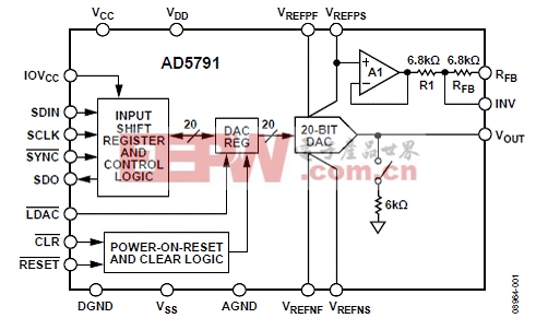
图1.AD5791方框图
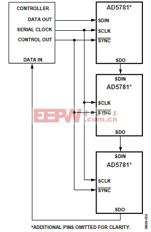
图2.AD5791菊花链接方框图

图3.AD5791典型应用电路图
EVAL-AD5791评估板
The EVAL-AD5791 is a full-featured evaluation board, designed to allow the user to easily evaluate all features of the AD5791 voltage output, 20-bit DAC. The AD5791 pins are accessible at on-board connectors for external connection. The board can be controlled by two means, via the on-board connector (J6) or via the system development platform connector (J3). The SDP board allows the evaluation board to be controlled through the USB port of a Windows? XP (SP2 or later) or Vista (32-bit) based PC using the AD5791 evaluation software.
EVAL-AD5791评估板主要特性:
Full-featured evaluation board for the AD5791
Link options
PC control in conjunction with Analog Devices, Inc., system development platform
PC software for control
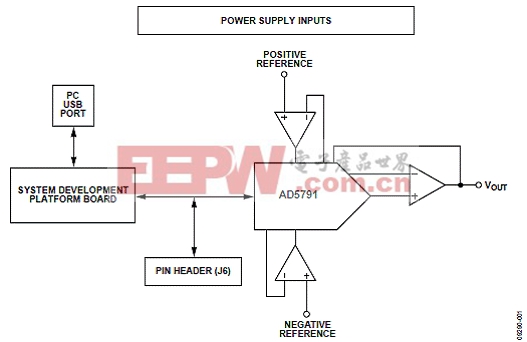
图4.EVAL-AD5791评估板连接框图
EVALUATION BOARD SCHEMATICS AND ARTWORK
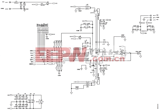
图5.EVAL-AD5791评估板电路图(1)
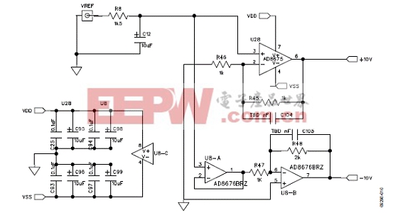
图6.EVAL-AD5791评估板基准电压电路图
图7.EVAL-AD5791评估板SDP板连接器电路
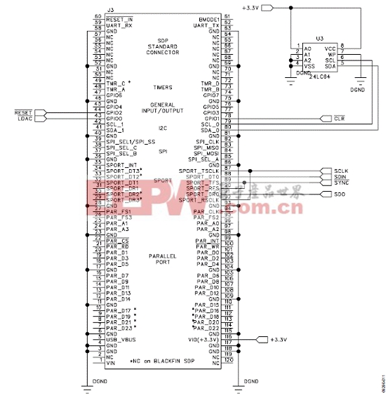
图8.EVAL-AD5791评估板元件布局图
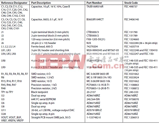
EVAL-AD5791评估板材料清单(BOM):
更多医疗电子信息请关注:21ic医疗电子频道


评论