Renesas V850ES-Jx3 移动心电图(ECG)解决方案
Renesas 公司的V850ES-Jx3 系列32位MCU包括V850ES/JC3-L系列和V850ES/JE3-L系列,集成了V850ES CPU内核和外设功能如ROM/RAM,定时器/计数器,串行接口,ADC,DAC,主要用在数码相机,电表,移动终端,数字家用电器和其它消费类电子.本文介绍了V850ES-Jx3 系列主要特性,方框图,以及移动心电图(ECG)系统框图和移动心电图(ECG)推荐的元件.
The V850ES/Jx3 microcontrollers are equipped with a high-capacity memory of 1 MB. Naturally furnished with functional interchangeability and pin interchangeability with the V850ES/Jx2 microcontrollers and capable of appropriating their development environment as well, the V850ES/Jx3 devices are capable of realizing system acceleration with ease.
The newest arrival to the lineup is the V850ES/Jx3-L microcontroller, an ultra-low power-consuming version of the V850ES/JG2 microcontroller, with less than half of its power comsumption current. The V850ES/Jx3-L lineup has achieved an industry-leading nominal power/performance ratio (0.9 mW/MIPS, which comes in under the 1 mW marker according to the Dhrystone evaluation) and actual operating current of 13 mA typ. (at 20 MHz) .Moreover, microcontrollers built in USB (peripheral) function are added in this low power V850ES/Jx3-L product lineup.
The V850ES/JC3-L and V850ES/JE3-L are 32-bit single-chip microcontrollers that include the V850ES CPU core and peripheral functions such as ROM/RAM, timer/counters, serial interfaces, an A/D converter, a D/A converter.
In addition to high real-time response characteristics and 1-clock-pitch basic instructions, the V850ES/JC3-L and V850ES/JE3-L feature multiply instructions, saturated operation instructions, bit manipulation instructions, etc., realized by a hardware multiplier, as optimum instructions for digital servo control applications. Moreover, as a real-time control system, the V850ES/JC3-L and V850ES/JE3-L enable an extremely high cost-performance for applications that require super low power consumption, such as PC peripheral device, ECR peripheral device, and industrial instrument.
V850ES-Jx3 系列主要特性:
Minimum instruction execution time: 50 ns (operating on main clock (fXX) of 20 MHz: VDD = 2.7 to 3.6 V)
200 ns (operating on main clock (fXX) of 5 MHz: VDD = 2.2 to 3.6 V)
30.5 s (operating on subclock (fXT) of 32.768 kHz)
General-purpose registers: 32 bits 32 registers
CPU features: Signed multiplication (16 16 →32): 1 to 2 clocks
Signed multiplication (32 32 →64): 1 to 5 clocks
Saturated operations (overflow and underflow detection functions included)
Most instructions can be executed in 1 clock cycle by using 32-bit RISC-based 5-stage pipeline architecture
Instruction fetching from internal ROM and accessing internal RAM for data can be
executed separately, by using Harvard architecture
High code efficiency achieved by using variable length instructions
32-bit shift instruction: 1 clock cycle
Bit manipulation instructions
Load/store instructions with long/short format
Memory space: 64 MB of linear address space (for programs and data)
Internal memory: RAM: 8/16 KB
Flash memory: 16/32/64/128/256 KB
Interrupts and exceptions: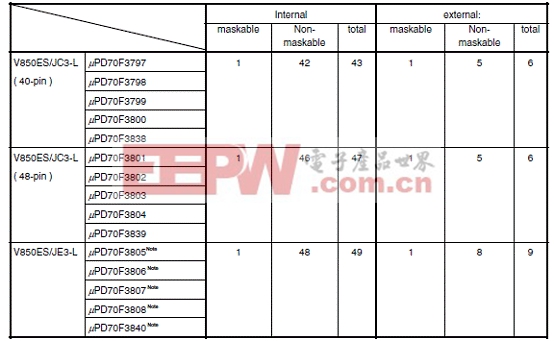
Ports: I/O ports: 27/34/50
Timer function: 16-bit interval timer M (TMM): 1 channel
16-bit timer/event counter P (TMP): 6 channels
16-bit timer/event counter Q (TMQ): 1 channel
Watch timer: 1 channel
Watchdog timer: 1 channel
Real-time counter: 1 channel
Real-time output port: 6 bits 1 channel
Serial interface: For details about the number of incorporated channels, Asynchronous serial interface A (UARTA)
Clocked serial interface B (CSIB)
I2C bus interface (I2C)






评论