用电子表格设计RTD接口

使用电子表格和一些简单的数学方法,将线性化接口设计成非线性RTD。
本文引用地址:https://www.eepw.com.cn/article/193527.htmRTD(电阻温度检测器)是高精度设计的首选传感器。RTD虽然在0到100°C的有限温区内近似为线性,但随着测量温度的范围逐渐加宽,这些传感器的电阻非线性呈现出轻微但逐渐增大的趋势。因此,在扩大的温度范围里,如果为使系统实现高精度,曲线拟合是必要的。避免RTD传感器非线性特征的一个方法是,在其他信号处理之前设计类似硬件实现曲线拟合运算。这个方法特别适用于价格低和器件数少,和微处理器设计不可行的情况。器件数少对小PCB(印制板)管脚有额外的好处。
最常用的RTD由0°C 100Ω的铂电阻制造,金属纯度导致它们符合标准带正温系数α为0.00385Ω/Ω/°C的欧洲曲线。不常用但仍可用的稍高金属纯度RTD。这些RTD有0.00392Ω/Ω/°C的α,符合美国曲线。图1电路使用标准RTD测量0到350°C的扩展温区,输出0到3.5V的电压,全程系统精度高于0.5°C。下面的线性方程表示了这个传感器系统:
![]()
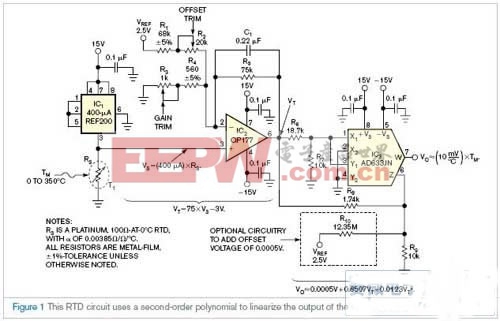
IC1为管脚可配置型,通过接地传感器T1驱动400µA的恒定电流。用这个水平的电流
驱动T1——“零功率”工作——保持传感器中电路消耗的最差功率小于40µW,减少对二阶效应的自热误差(参考文献1)。用电流源驱动RTD也保持其固有的非线性,允许表示传感器的输出电压VS为400µA×RS,在这里RS为传感器电阻。
IC2最初通过先缩放输出电压,再将结果偏置的方法,实现传感器输出的信号调理,所以VT稍大于350°C下的3.5V输出,VT在0°C下为0V。在线性化处理之前加入增益和偏置,减少了曲线拟合电路的负担,且有助于满足系统的精度指标。C1与R5结合实现了单极约10Hz的低通滤波,消除电源噪声。下面的公式描述了IC2的性能和其伴随电路:VT=75VS–3V。
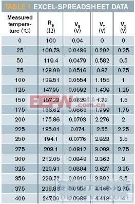
其次,Excel表格建立了电压VT和系统输出VO之间的非线性数学关系(表1)。表格有17个温度条目,从0°C到400°C,以25°C递增。使用数组扩充超过预设的350°C测量温度范围,减少非线性系统的端误差。RS值——来源于标准RTD电阻随温度表——方程用于计算VS和VT。VT和VO的列对于线性化电路分别为输入和输出信号;使用Excel的XY分散特性制图。使用Excel的趋势特征建立了下面的公式,所需曲线拟合电路的数学表达将传感器输出线性化:VO=0.0005V+0.8597VT+0.0123VT2。IC3和四个1%误差的电阻或随意五个电阻实现二阶多项式:VO=a+bVT+cVT2,在这里a为偏置量,b为线性系数,C为二次项系数。
曲线拟合电路的设计从画出IC3的四个输入建立二次项开始,也就是说通过内部1/10V的比例缩放芯片输出。然后,经比较发现系数C必须为0.0123。因为R6和R7的分压器削弱了信号VT,可用下面的公式表示系数:

选择R7的值为——本设计为10 kΩ——然后使用上述公式计算R6。
电阻R8、R9和随意无源加法器R10建立偏置项a和线性系数b。将无源加法器的输出直接连到IC3的管脚6,Z输入,其将偏置和线性项相加到二次项形成管脚7的系统响应。再次比较这些项,注意到偏置项必须等于0.0005V。偏置项仅为0.5mV,消除它会增加约0.05°C的误差,所以可在一开始忽略它。随后,因为线性项的系数必须等于0.8507,首先选择R9合适的值,使用下面的公式计算R8:b=R9/(R8+R9)。
如果希望设计可选电路和包含偏置项,其为无源加法器的一部分,选择稳定的2.5V参考为VREF,计算并联结果R8//R9=REQ(R8与R9并联的等效电阻),使用下面的分压器公式计算R10:a=(REQ/(R9+REQ))VREF。
为校准电路,用精密十进制电阻箱取代传感器。设置电阻箱模拟0°C,调整IC3管脚7的R2偏置端使输出为0V。其次,设置电阻箱模拟350°C,调整R3的增益端使输出为3.5V。重复这个端调整步骤的顺序直到两个点都确定。如图1电路——包括可选电路——显示了250°C时最差测量误差为2.504V的0.16%,或0.4°C。没有可选电路时测试电路——参考电压和R10——显示精度上没有显著改善。
英文原文:
Design an RTD interface with a spreadsheet
Using a spreadsheet and some simple math, you can design a linearizing interface to a non-linear RTD.
Robert S Villanucci, Wentworth Institute of Technology, Boston; Edited by Charles H Small and Fran Granville -- EDN, 2/7/2008
RTDs (resistance-temperature detectors) are the preferred sensor choices for designs requiring precision. Although RTDs are approximately linear over the limited temperature range of 0 to 100°C, these sensors exhibit a slight but progressively more nonlinear temperature-versus-resistance characteristic as the measurement range widens. Consequently, over an extended span, curve fitting is necessary if the system is to achieve a high level of precision. One way to obviate the nonlinear characteristic of an RTD sensor is to design analog hardware to perform the curve-fitting mathematics before any additional signal processing occurs. This approach is especially attractive if you can keep both cost and component count low and if a microprocessor-driven design is not feasible. With low component count comes the added benefit of a small PCB (printed-circuit-board) footprint.
The most popular RTDs are made from platinum with a resistance value of 100Ω at 0°C and a metal purity that allows them to follow a standard European curve with a positive-temperature coefficient, α, equal to 0.00385Ω/Ω/°C. Less popular but still common are RTDs with a slightly higher metal purity. These RTDs have α of 0.00392Ω/Ω/°C and follow the US curve. The circuit in Figure 1 uses a standard RTD to measure temperature over the extended range of 0 to 350°C, an output voltage of 0 to 3.5V, and overall system accuracy greater than 0.5°C. The following linear equation expresses this sensor system:
IC1 is pin-configured to drive a constant current of 400 µA through the grounded sensor, T1. Driving T1 with this level of current—“zero-power” operation—keeps the worst-case power that the circuit dissipates in the sensor to less than 40 µW and reduces the self-heating errors to a second-order effect (Reference 1). Also, driving the RTD with a current source preserves its intrinsic nonlinearity and allows you to express the sensor’s output voltage, VS, as: 400 µA×RS, where RS is the resistance of the sensor.
IC2 initially signal-conditions the sensor’s output by first scaling the output voltage and then offsetting the result so that VT is slightly larger than the 3.5V output at 350°C and that VT equals 0V at 0°C. Adding gain and offset before linearization places less of a burden on the curve-fitting circuitry and helps to meet the system’s precision specification. The combination
of C1 and R5 implements a lowpass filter with a pole at approximately 10 Hz to remove power-supply noise. The following term describes the performance of IC2 and its accompanying circuitry: VT=75VS–3V.
Next, an Excel spreadsheet creates the nonlinear-mathematical relationship between the voltage, VT, and the system output, VO (Table 1). The spreadsheet features 17 temperature entries—starting at 0°C, increasing in increments of 25°C, and ending at 400°C—for the measured temperature. Using a data set that extends beyond the intended measurement range of 350°C can reduce end errors in nonlinear systems. Values for RS—which you derive from a standard RTD-resistance-versus-temperature table—and the equations allow you to compute VS and VT. The VT and VO columns are the input and output signals, respectively, for the linearization circuitry; you chart them using Excel’s XY-scatter feature. You can use Excel’s Trendline feature to create the following equation, the mathematical representation of the curve-fitting circuitry you need to linearize the sensor’s output: VO=0.0005V+0.8597VT+0.0123VT 2. IC3 and four 1%-tolerant resistors or, optionally, five resistors implement a second-order polynomial: VO=a+bVT+cVT 2, where a is the offset term, b is the linear coefficient, and c is the square-term coefficient.
The curve-fitting-circuit design begins by first wiring the four inputs of IC3 to create a positive square term that is scaled at the chip’s output by an internal scale factor of 1/10V. Then, comparing terms, you find that the coefficient, c, must equal 0.0123. Because R6 and R7 form a voltage divider that attenuates the signal, VT, you can express the coefficient with the following equation:
Select a value for R7—10 kΩ for this design—and then use the preceding equation to find the value for R6.
Resistors R8, R9, and, optionally, R10 form a passive adder to create the offset term, a, and the linear coefficient, b. You apply the output of the passive
adder directly to the Z input, Pin 6 of IC3, which adds the offset and linear terms to the square term to form the system response at Pin 7. Again comparing these terms, note that the offset term must equal 0.0005V. The offset term is only 0.5 mV, and eliminating it would add an error of approximately 0.05°C, so you can initially neglect it. Then, because the linear term’s coefficient, b, must equal 0.8507, you first select a suitable value for R9 and use the following equation to solve for R8: b=R9/(R8+R9).
If you wish to design the optional circuitry and include the offset term, which is part of the passive adder, choose a stable 2.5V reference for VREF, calculate the parallel combination of R8//R9=REQ (the equivalent resistance of R8 in parallel with R9), and solve for R10 using the following voltage-divider equation: a=(REQ/(R9+REQ))VREF.
To calibrate this circuit, replace the sensor with a precision decade box. Set the decade box to simulate 0°C and adjust the offset trim of R2 for an output of 0V at Pin 7 of IC3. Next, set the decade box to simulate 350°C and adjust the gain trim of R3 for an output of 3.5V. Repeat this sequence of trim steps until both points are fixed. The circuit in Figure 1—which includes optional circuitry—exhibits a worst-case measurement error at 250°C and 2.504V of 0.16%, or 0.4°C. Testing the circuit without the optional circuitry—the reference voltage and R10 —shows no discernible improvement in precision.
Reference
“IC Generates Second-Order Polynomial,” Electronic Design, Aug 5, 1993.

cvt相关文章:cvt原理
电流变送器相关文章:电流变送器原理
评论