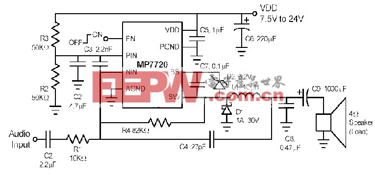
Freescale MC56F8257数字信号控制器开发方案
• Parallel instruction set with unique DSP addressing modes
• Hardware DO and REP loops
• Instruction set supports DSP and controller functions
• Controller-style addressing modes and instructions for compact code
• Efficient C compiler and local variable support
• Software subroutine and interrupt stack with depth limited only by memory
•JTAG/enhanced on-chip emulation (EOnCE) for unobtrusive, processor speed–independent, real-time debugging
Operation Range
• 3.0 V to 3.6 V operation (power supplies and I/O)
• From power-on-reset: approximately 2.7 V to 3.6 V
• Ambient temperature operating range: –40 ℃ to +105 ℃
Memory
• Dual Harvard architecture that permits as many as three simultaneous accesses to program and data memory
• 48 KB (24K x 16) to 64 KB (32K x 16) on-chip flash memory with 2048 bytes (1024 x 16) page size
• 6 KB (3K x 16) to 8 KB (4K x 16) on-chip RAM with byte addressable
• EEPROM emulation capability using flash
• Support for 60 MHz program execution from both internal flash and RAM memories
• Flash security and protection that prevent unauthorized users from gaining access to the internal flash
Interrupt Controller
• Five interrupt priority levels
— Three user programmable priority levels for each interrupt source: Level 0, 1, 2
— Unmaskable level 3 interrupts include: illegal instruction, hardware stack overflow, misaligned data access, and SWI3 instruction Maskable level 3 interrupts include: EOnCE step counter, EOnCE breakpoint unit, and EOnCE trace buffer
— Lowest-priority software interrupt: level LP
• Nested interrupts: higher priority level interrupt request can interrupt lower priority interrupt subroutine
• Two programmable fast interrupts that can be assigned to any interrupt source
• Notification to system integration module (SIM) to restart clock out of wait and stop states
• Ability to relocate interrupt vector table
The masking of interrupt priority level is managed by the 56800E core.
Peripheral Highlights
• One Enhanced Flex Pulse Width Modulator (eFlexPWM) module
— Up to nine output channels
— 16-bit resolution for center aligned, edge aligned, and asymmetrical PWMs
— Each complementary pair can operate with its own PWM frequency based and deadtime values
– 4 Time base
– Independent top and bottom deadtime insertion
— PWM outputs can operate as complimentary pairs or independent channels
— Independent control of both edges of each PWM output
— 6-channel NanoEdge high resolution PWM
– Fractional delay for enhanced resolution of the PWM period and edge placement
– Arbitrary eFlexPWM edge placement - PWM phase shifting
– NanoEdge implementation: 520 ps PWM frequency resolution
— 3 Channel PWM with full Input Capture features
– Three PWM Channels - PWMA, PWMB, and PWMX
– Enhanced input capture functionality
— Support for synchronization to external hardware or other PWM
— Double buffered PWM registers
– Integral reload rates from 1 to 16
– Half cycle reload capability
— Multiple output trigger events can be generated per PWM cycle via hardware
— Support for double switching PWM outputs
— Up to four fault inputs can be assigned to control multiple PWM outputs
– Programmable filters for fault inputs
— Independently programmable PWM output polarity
— Individual software control for each PWM output
— All outputs can be programmed to change simultaneously via a FORCE_OUT event
— PWMX pin can optionally output a third PWM signal from each submodule
— Channels not used for PWM generation can be used for buffered output compare functions
— Channels not used for PWM generation can be used for input capture functions
— Enhanced dual edge capture functionality
— Option to supply the source for each complementary PWM signal pair from any of the following:
– Crossbar module outputs
– External ADC input, taking into account values set in ADC high and low limit registers
• Two independent 12-bit analog-to-digital converters (ADCs)
— 2 x 8 channel external inputs Built-in x1, x2, x4 programmable gain pre-amplifier
— Maximum ADC clock frequency: up to 10 MHz
– Single conversion time of 8.5 ADC clock cycles (8.5 x 100 ns = 850 ns)


评论