AD9644:14位串行模数转换器应用详解(原创)

AD9644是一款14位双通道模数转换器(ADC),配有一个高速串行输出接口,采样速度可为80MSPS或155MSPS。这款双通道ADC内核采用多级、差分流水线架构,并集成了输出纠错逻辑。每个ADC均具有宽带宽、差分采样保持模拟输入放大器,支持用户可选的各种输入范围。集成基准电压源可简化设计。占空比稳定器可用来补偿ADC时钟占空比的波动,使转换器保持出色的性能。
本文引用地址:https://www.eepw.com.cn/article/258524.htm控制理论
The AD9644 dual-core analog-to-digital converter (ADC) can be used for diversity reception of signals, in which the ADCs are operating identically on the same carrier but from two separate antennae. The ADCs can also be operated with independent analog inputs. The user can sample any fS/2 frequency segment from dc to 250 MHz, using appropriate low-pass or band-pass filtering at the ADC inputs with little loss in ADC performance.
In nondiversity applications, the AD9644 can be used as a base-band or direct downconversion receiver, in which one ADC is used for I input data, and the other is used for Q input data.
Synchronization capability is provided to allow synchronized timing between multiple devices. Programming and control of the AD9644 are accomplished using a 3-wire SPI-compatible serial interface.
模数转换器结构
The AD9644 architecture consists of a dual front-end sample-and-hold circuit, followed by a pipelined, switched-capacitor ADC. The quantized outputs from each stage are combined into a final 14-bit result in the digital correction logic. The pipelined architecture permits the first stage to operate on a new input sample and the remaining stages to operate on the preceding samples. Sampling occurs on the rising edge of the clock.
Each stage of the pipeline, excluding the last, consists of a low resolution flash ADC connected to a switched-capacitor digital-to-analog converter (DAC) and an interstage residue amplifier (MDAC). The MDAC magnifies the difference between the recon-structed DAC output and the flash input for the next stage in the pipeline. One bit of redundancy is used in each stage to facilitate digital correction of flash errors. The last stage simply consists of a flash ADC.
The input stage of each channel contains a differential sampling circuit that can be ac- or dc-coupled in differential or single-ended modes. The output staging block aligns the data, corrects errors, and passes the data to the output buffers. The output buffers are powered from a separate supply, allowing digital output noise to be separated from the analog core. During power-down, the output buffers go into a high impedance state.
模拟输入注意事项
The analog input to the AD9644 is a differential switched-capacitor circuit that has been designed for optimum performance while processing a differential input signal.
The clock signal alternatively switches the input between sample mode and hold mode (see Figure 1). When the input is switched into sample mode, the signal source must be capable of charging the sample capacitors and settling within ½ of a clock cycle.
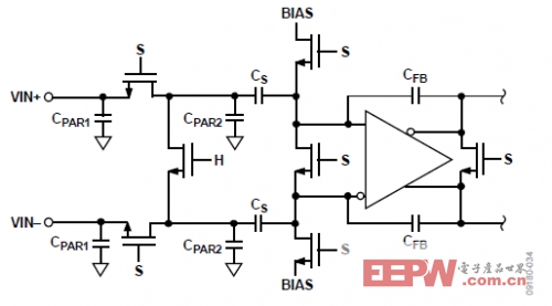
Figure 1
A small resistor in series with each input can help reduce the peak transient current required from the output stage of the driving source. A shunt capacitor can be placed across the inputs to provide dynamic charging currents. This passive network creates a low-pass filter at the ADC input; therefore, the precise values are dependent on the application.
In intermediate frequency (IF) undersampling applications, any shunt capacitors or series resistors should be reduced since the input sample capacitor is unbuffered. In combination with the driving source impedance, the shunt capacitors limit the input bandwidth. Refer to the AN-742 Application Note, Frequency Domain Response of Switched-Capacitor ADCs; the AN-827 Application Note, A Resonant Approach to Interfacing Amplifiers to Switched-Capacitor ADCs; and the Analog Dialog article, “Transformer-Coupled Front-End for Wideband A/D Converters,” for more information on this subject (refer to www.analog.com).
For best dynamic performance, the source impedances driving VIN+ and VIN− should be matched, and the inputs should be differentially balanced.
输入模式
The analog inputs of the AD9644 are not internally dc biased. In ac-coupled applications, the user must provide this bias externally. Setting the device so that VCM = 0.5 × AVDD (or 0.9 V) is recommended for optimum performance. An on-board common-mode voltage reference is included in the design and is available from the VCMA and VCMB pins. Using the VCMA and VCMB outputs to set the input common mode is recommended. Optimum performance is achieved when the common-mode voltage of the analog input is set by the VCMA and VCMB pin voltages (typically 0.5 × AVDD). The VCMA and VCMB pins must be decoupled to ground by a 0.1 μF capacitor. This decoupling capacitor should be placed close to the pin to minimize the series resistance and inductance between the part and this capacitor.
差分输入配置
Optimum performance is achieved while driving the AD9644 in a differential input configuration. For baseband applications, the AD8138, ADA4937-2, and ADA4938-2 differential drivers provide excellent performance and a flexible interface to the ADC.
The output common-mode voltage of the ADA4938-2 is easily set with the VCM pin of the AD9644 (see Figure 2), and the driver can be configured in a Sallen-Key filter topology to provide band limiting of the input signal.
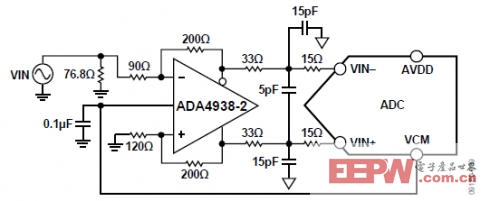
Figure 2. Differential Input Configuration Using the ADA4938-2
For baseband applications in which SNR is a key parameter, differential transformer coupling is the recommended input configuration. An example is shown in Figure 3. To bias the analog input, the VCM voltage can be connected to the center tap of the secondary winding of the transformer.
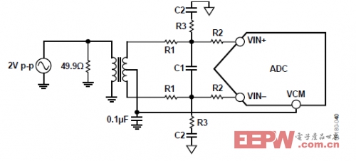
Figure 3. Differential Transformer-Coupled Configuration
The signal characteristics must be considered when selecting a transformer. Most RF transformers saturate at frequencies below a few megahertz (MHz). Excessive signal power can also cause core saturation, which leads to distortion.
At input frequencies in the second Nyquist zone and above, the noise performance of most amplifiers is not adequate to achieve the true SNR performance of the AD9644. For applications in which SNR is a key parameter, differential double balun coupling is the recommended input configuration (see Figure 4). In this configuration, the input is ac-coupled and the VCM is provided to each input through a 33 Ω resistor. These resistors compensate for losses in the input baluns to provide a 50 Ω impedance to the driver.
In the double balun and transformer configurations, the value of the input capacitors and resistors is dependent on the input fre-quency and source impedance. Based on these parameters the value of the input resistors and capacitors may need to be adjusted or some components may need to be removed. Table 9 displays recommended values to set the RC network for different input frequency ranges. However, these values are dependent on the input signal and bandwidth and should be used only as a starting guide. Note that the values given in Table 9 are for each R1, R2, C2, and R3 component shown in Figure 3 and Figure 4.
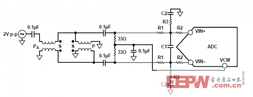
Figure 4
An alternative to using a transformer-coupled input at frequencies in the second Nyquist zone is to use the AD8376 variable gain amplifier. An example drive circuit including a band-pass filter is shown in Figure 5. See the AD8376 data sheet for more information.
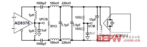
Figure5
推荐阅读:
AD9644:14位串行模数转换器概述

评论