LatticeLatticeECP3PCIE桥接解决方案

The LatticeECP3™ (EConomy Plus Third generation) family of FPGA devices is optimized to deliver high perfor-mance features such as an enhanced DSP architecture, high speed SERDES and high speed source synchronous interfaces in an economical FPGA fabric. This combination is achieved through advances in device architecture and the use of 65nm technology making the devices suitable for high-volume, high-speed, low-cost applications. The LatticeECP3 device family expands look-up-table (LUT) capacity to 149K logic elements and supports up to 586 user I/Os. The LatticeECP3 device family also offers up to 320 18x18 multipliers and a wide range of parallel I/O standards. The LatticeECP3 FPGA fabric is optimized with high performance and low cost in mind. The LatticeECP3 devices utilize reconfigurable SRAM logic technology and provide popular building blocks such as LUT-based logic, distrib-uted and embedded memory, Phase Locked Loops (PLLs), Delay Locked Loops (DLLs), pre-engineered source synchronous I/O support, enhanced sysDSP slices and advanced configuration support, including encryption and dual-boot capabilities. The pre-engineered source synchronous logic implemented in the LatticeECP3 device family supports a broad range of interface standards, including DDR3, XGMII and 7:1 LVDS. The LatticeECP3 device family also features high speed SERDES with dedicated PCS functions. High jitter toler-ance and low transmit jitter allow the SERDES plus PCS blocks to be configured to support an array of popular data protocols including PCI Express, SMPTE, Ethernet (XAUI, GbE, and SGMII) and CPRI. Transmit Pre-empha-sis and Receive Equalization settings make the SERDES suitable for transmission and reception over various forms of media. The LatticeECP3 devices also provide flexible, reliable and secure configuration options, such as dual-boot capa-bility, bit-stream encryption, and TransFR field upgrade features. The Lattice Diamond™ and ispLEVER® design software allows large complex designs to be efficiently imple-mented using the LatticeECP3 FPGA family. Synthesis library support for LatticeECP3 is available for popular logic synthesis tools. Diamond and ispLEVER tools use the synthesis tool output along with the constraints from its floor planning tools to place and route the design in the LatticeECP3 device. The tools extract the timing from the routing and back-annotate it into the design for timing verification. Lattice provides many pre-engineered IP (Intellectual Property) modules for the LatticeECP3 family. By using these configurable soft core IPs as standardized blocks, designers are free to concentrate on the unique aspects of their design, increasing their productivity.
LatticeECP3器件主要特性:
Higher Logic Density for Increased System Integration
•17K to 149K LUTs
•116 to 586 I/Os
Embedded SERDES
•150 Mbps to 3.2 Gbps for Generic 8b10b, 10-bit SERDES, and 8-bit SERDES modes
•Data Rates 230 Mbps to 3.2 Gbps per channel for all other protocols
•Up to 16 channels per device: PCI Express, SONET/SDH, Ethernet (1GbE, SGMII, XAUI), CPRI, SMPTE 3G and Serial RapidIO
sysDSP™•Fully cascadable slice architecture
•12 to 160 slices for high performance multiply and accumulate
•Powerful 54-bit ALU operations
•Time Division Multiplexing MAC Sharing
•Rounding and truncation
•Each slice supports
Flexible Memory Resources
•Up to 6.85Mbits sysMEM™Embedded Block RAM (EBR)
•36K to 303K bits distributed RAM
sysCLOCK Analog PLLs and DLLs
•Two DLLs and up to ten PLLs per device
Pre-Engineered Source Synchronous I/O
•DDR registers in I/O cells
•Dedicated read/write levelling functionality
•Dedicated gearing logic
•Source synchronous standards support
•Dedicated DDR/DDR2/DDR3 memory with DQS support
•Optional Inter-Symbol Interference (ISI) correction on outputs
Programmable sysI/O™Buffer Supports Wide Range of Interfaces
•On-chip termination
•Optional equalization filter on inputs
•LVTTL and LVCMOS 33/25/18/15/12
•SSTL 33/25/18/15 I, II
•HSTL15 I and HSTL18 I, II
•PCI and Differential HSTL, SSTL
•LVDS, Bus-LVDS, LVPECL, RSDS, MLVDS
Flexible Device Configuration
•Dedicated bank for configuration I/Os
•SPI boot flash interface
•Dual-boot images supported
•Slave SPI
•TransFR™I/O for simple field updates
•Soft Error Detect embedded macro
System Level Support
•IEEE 1149.1 and IEEE 1532 compliant
•Reveal Logic Analyzer
•ORCAstra FPGA configuration utility
•On-chip oscillator for initialization general use
•1.2V core power supply
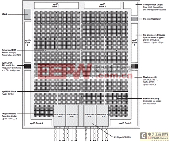
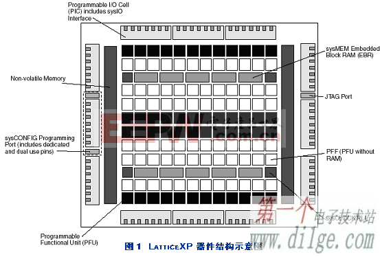
图1. LatticeECP3-35 器件简化框图
As PCI Express applications have emerged, the LatticeECP3™ FPGA family has become a well-suited solution for many system designs. The features of the LatticeECP3 PCI Express Solutions Board can assist engineers with rapid-prototyping and testing their designs. The board is an enhanced form-factor of the PCI Express add-in card specification. It allows for full x1 form-factor compliance and x4 is available for demonstration purposes with some non-standard form-factor issues. The flexibility to use the same board to demonstrate both x1 and x4 configurations is accomplished by simply changing the mounting hardware. The board has several debugging and analyzing fea-tures for complete evaluation of the LatticeECP3 device. This guide is intended to be referenced in conjunction with evaluation design tutorials to demonstrate the LatticeECP3 FPGA.
This user’s guide describes the LatticeECP3 PCI Express Solutions Board featuring the LatticeECP3 LFE3-95EA-FN672 FPGA. The stand-alone evaluation board provides a functional platform for development and rapid prototyp-ing of applications that require high-speed SERDES interfaces to demonstrate PCI Express capabilities using an add-on card form-factor. The board is manufactured using standard FR4 dielectric and through-hole vias. The nom-inal impedance is 50-ohm for single-ended traces and 85-ohm for differential traces.
• PCI Express x1 and x4 edge connector interfaces
• Allows demonstration of PCI Express (x 1and x4) interfaces
– x1 is form-factor compliant and will fit a standard PC-equipped PCI Express motherboard socket
– x4 is non-compliant but will demonstrate x4 functionality by a simple change to the hardware
• Allows control of SERDES PCS registers using the Serial Client Interface (ORCAstra) • On-board Boot Flash
– Both Serial SPI Flash and Parallel Flash via MachXO™ programming bridge
• Shows interoperation with a high performance DDR2 memory component
• Includes driver based “run-time” device configuration capability via ORCAstra or PCI Express
• Switches, LEDs, displays for demo purposes
• Input connection for lab-power supply
• Power connections and power sources
• ispVM™ programming support
• On-board and external reference clock sources
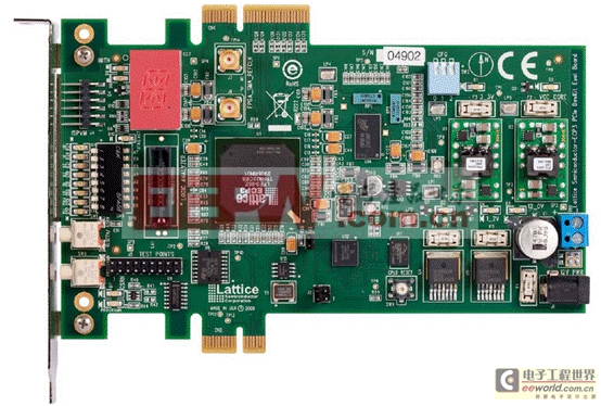
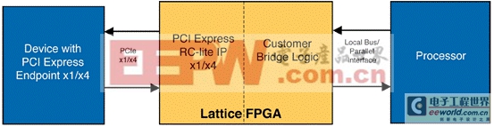
图3.PCI Express桥接解决方案框图
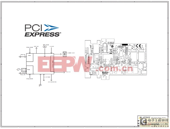
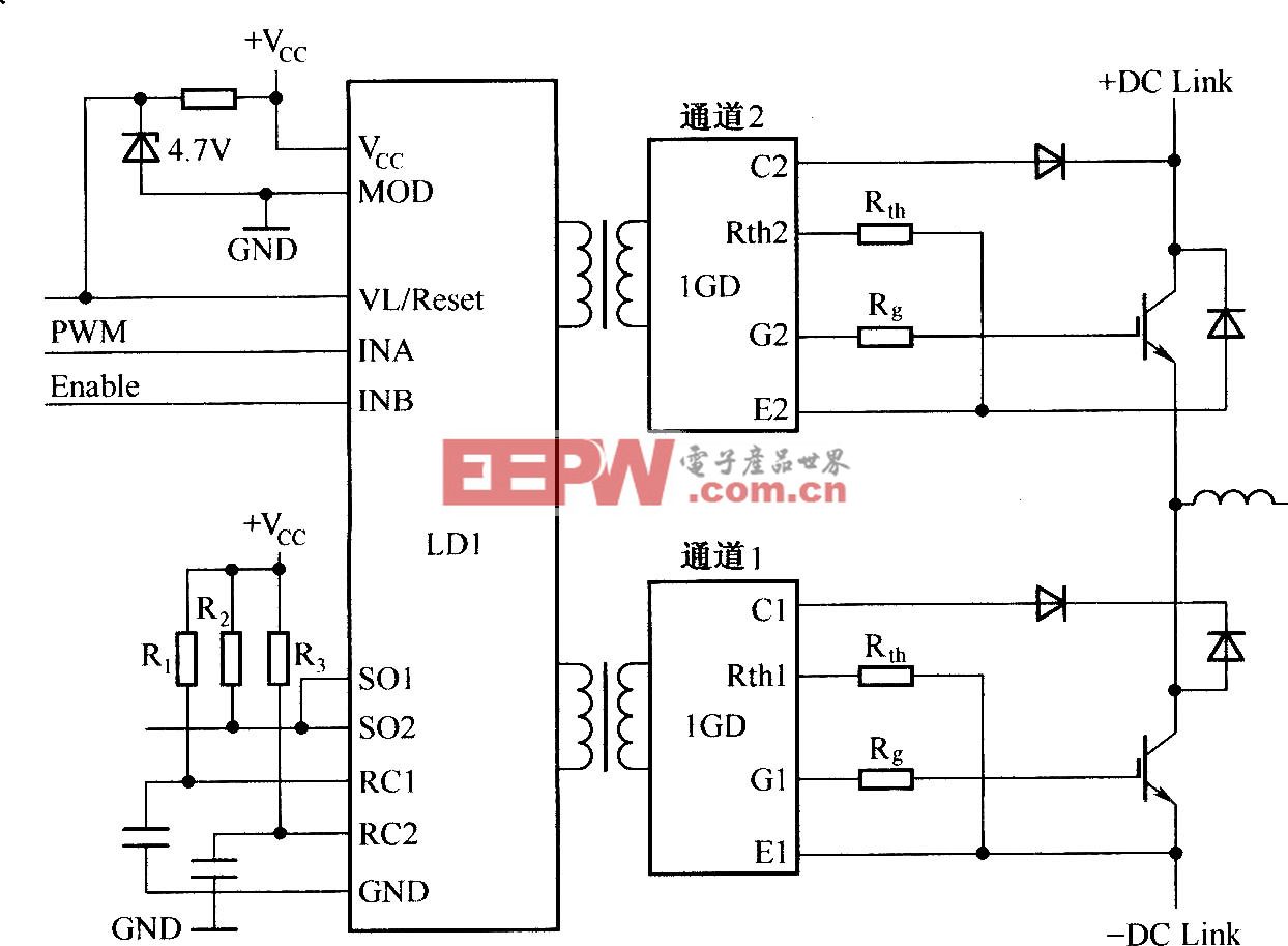
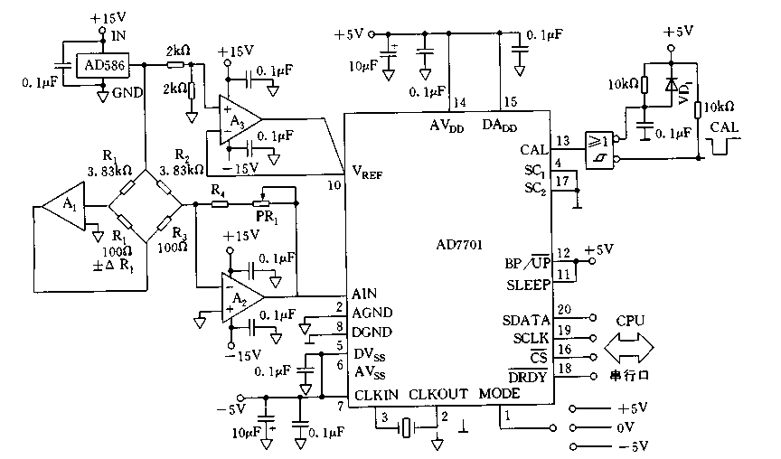
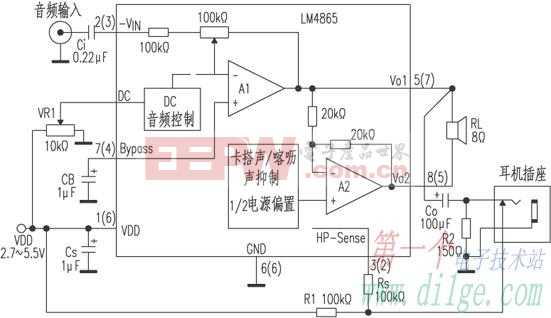
图4.EB43 PCI Express桥接评估板电路图(1)
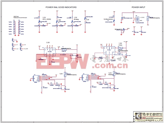
图5.EB43 PCI Express桥接评估板电路图(2)
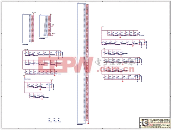
图6.EB43 PCI Express桥接评估板电路图(3)
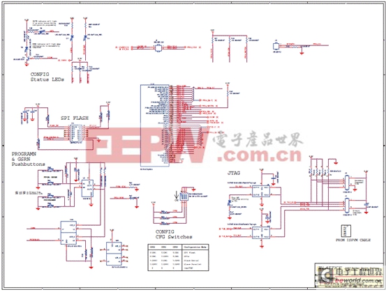
图7.EB43 PCI Express桥接评估板电路图(4)
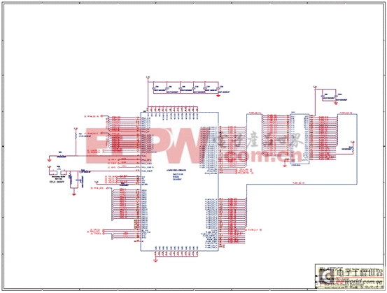
图8.EB43 PCI Express桥接评估板电路图(5)
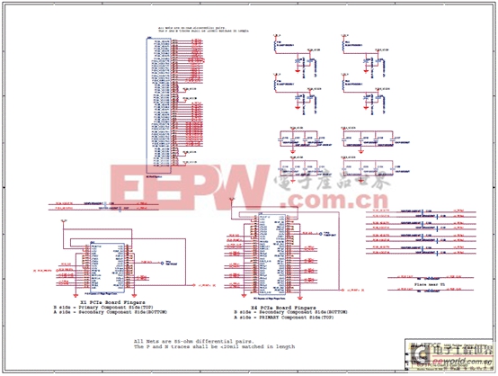
图9.EB43 PCI Express桥接评估板电路图(6)
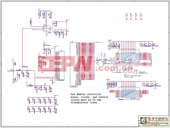
图10.EB43 PCI Express桥接评估板电路图(7)
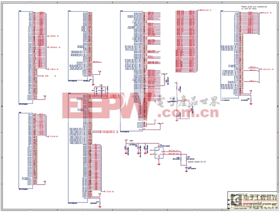
图11.EB43 PCI Express桥接评估板电路图(8)
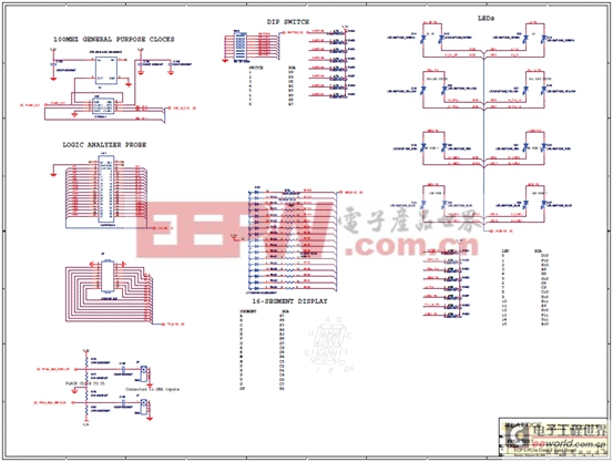
图12.EB43 PCI Express桥接评估板电路图(9)
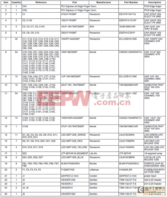
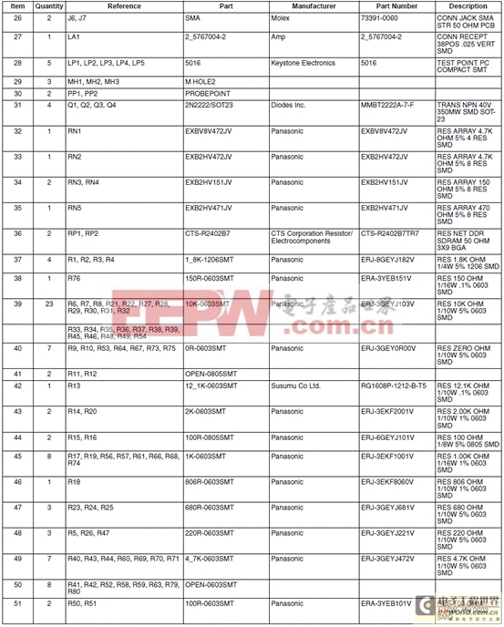
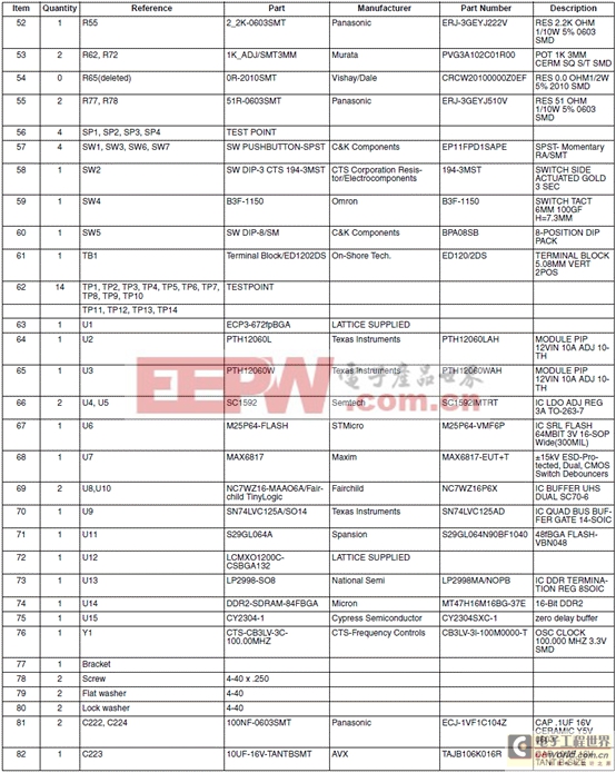
EB43 PCI Express桥接评估板材料清单(BOM):

电路图符号相关文章:电路图符号大全

评论