基于fpga二维小波变换核的实时可重构电路
2. 软件部分
本文引用地址:http://www.eepw.com.cn/article/266432.htm(1)bit n 的生成过程
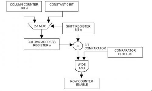
图 7 输出地址bit n 的生成
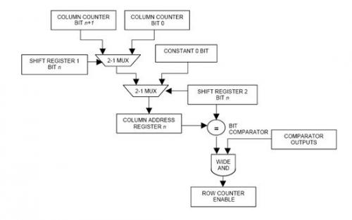
图 8 输入地址bit n 的生成
(2)部分代码
1 #Configuring F and G look-up tables with JBits
/* define row and column values */
int row = 5; int col = 4;
/* define logic function for F LUT */
int[] F_LUT_Vals = Expr.F_LUT(“~(F1&F2&F3&F4)”);
/* define logic function for G LUT */
int[] G_LUT_Vals = Expr.G_LUT(“~(F1|F2|F3|F4)”);
/* set the F LUT value for slice 0 */
jbits.set(row, col, LUT.SLICE0_F, F_LUT_Vals);
/* set the G LUT value for slice 1 */
jbits.set(row, col, LUT.SLICE1_G, G_LUT_Vals);
2 #: Adding and configuring an OutputCore
/* create a signal to run to the cross bar pins on the Slaac1V X2 */
Bus XBar = new Bus("XP_XBAR", null, 20);
/* create a new board */
Slaac1VBoard slaac1V = new Slaac1VBoard("SLAAC1V");
/* add a cross bar output core to slaac1V board instance */
int XBarOutput = slaac1V.addOutput(Xbar.getName(), XBar);
/* configure the IOB resources output operation */
slaac1V.setOutputInvertT(XBarOutput, true);
/* implement the slaac1V board */
slaac1V.implement(0, "slaac1V.ucf");
3 #Code showing how Slaac1V SRAMs are distinguished through signal names.
/* define memory signals for Slaac1V X2 memories 0 and 1 */
Bus addr[] = new Bus[2];
Bus data[] = new Bus[2];
/* memory address */
addr[0] = new Bus("XP_MEM0_ADDR", null, 18); /* SRAM 0 */
addr[1] = new Bus("XP_MEM1_ADDR", null, 18); /* SRAM 1 */
/* memory data */
data[0] = new Bus("XP_MEM0_DATA", null, 12); /* SRAM 0 */
data[1] = new Bus("XP_MEM1_DATA", null, 12); /* SRAM 1 */
4 #AdderTree input index computations and partitioning process
/* calculate the “parent” adder index */
int log = (int) Math.ceil(Math.log((double)range)/Math.log(2.0));
int parentAdder = low + (int) Math.pow(2.0,log - 1);
/* calculate the right sided adder input index */
range = high - parentAdder;
log = (int) Math.ceil(Math.log((double)range)/Math.log(2.0));
int RHSIndex = ((int) Math.pow(2.0, log - 1)) + parentAdder;
/* calculate the left sided adder input index */
range = parentAdder - low;
log = (int) Math.ceil(Math.log((double)range)/Math.log(2.0));
int LHSIndex = ((int) Math.pow(2.0, log - 1)) + low;
/* partition left hand side of parent adder recursively */
AIndex[parentAdder - 1] = LHSIndex - 1;
deriveAdderTree(low, parentAdder);
/* partition right hand side of parent adder recursively */
if (RHSIndex != parentAdder)
{
BIndex[parentAdder - 1] = RHSIndex - 1;
deriveAdderTree(parentAdder, high);
}
else /* required if there is an odd number of tree inputs */
{
BIndex[parentAdder - 1] = treeInPort.length - 1;
}
5 # Slaac1VBoard.java code
public class Slaac1VBoard extends Board
{
public Slaac1VBoard(String name) throws CoreParameterException
{
super(name);
setXCVPackage(xcvPackage);
setGCLK(GCLK);
};
private XCVPackage xcvPackage[] =
{
new xcv1000_fg680(), new xcv1000_fg680(), new xcv1000_fg680()
};
private static int GCLK = 2;
}; /* end of Slaac1V board class. */
3.2 需要的开发平台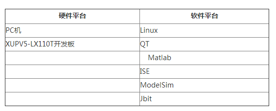


评论