IGLOO的FPGA构成的马达控制方案
本文介绍了IGLOO系列主要特性和优势,IGLOO系列架构框图以及采用AGL125的马达控制子板主要特性,步进马达控制逻辑方框图,BLDC马达控制逻辑方框图以及马达控制子板电路图和材料清单。
Actel公司的IGLOO系列FPGA是采用Flash Freeze技术的低功耗闪存FPGA,它基于130nm闪存工艺,具有最低功耗,单片解决方案和小占位面积的封装,可重新编程以及丰富的其它特性,核电压1.2 V -1.5 V,支持低功耗和单电压系统工作,Flash Freeze模式的功耗为5uW,系统门从15K到100万,多达144kb的双端口SRAM和多达300个用户I/O,可满足消费品,工业,医疗,汽车电子,计算,通信和军用航天领域的便携产品对低功耗的需要。
IGLOO系列主要特性和优势:
Low Power
• 1.2 V to 1.5 V Core Voltage Support for Low Power
• Supports Single-Voltage System Operation
• 5 μW Power Consumption in Flash*Freeze Mode
• Low Power Active FPGA Operation
• Flash*Freeze Technology Enables Ultra-Low Power Consumption while Maintaining FPGA Content
• Easy Entry to / Exit from Ultra-Low Power Flash*Freeze Mode
High Capacity
• 15 k to 1 Million System Gates
• Up to 144 kbits of True Dual-Port SRAM
• Up to 300 User I/Os
Reprogrammable Flash Technology
• 130-nm, 7-Layer Metal, Flash-Based CMOS Process
• Live-at-Power-Up (LAPU) Level 0 Support
• Single-Chip Solution
• Retains Programmed Design When Powered Off
• 250 MHz (1.5 V systems) and 160 MHz (1.2 V systems) System Performance
In-System Programming (ISP) and Security
• Secure ISP Using On-Chip 128-Bit Advanced Encryption Standard (AES) Decryption (except ARM®-enabled IGLOO® devices) via JTAG (IEEE 1532–compliant)†
• FlashLock® to Secure FPGA Contents
High-Performance Routing Hierarchy
• Segmented, Hierarchical Routing and Clock Structure
Advanced I/O
• 700 Mbps DDR, LVDS-Capable I/Os (AGL250 and above)
• 1.2 V, 1.5 V, 1.8 V, 2.5 V, and 3.3 V Mixed-Voltage Operation
• Bank-Selectable I/O Voltages—up to 4 Banks per Chip
• Single-Ended I/O Standards: LVTTL, LVCMOS 3.3 V / 2.5 V / 1.8 V / 1.5 V / 1.2 V, 3.3 V PCI / 3.3 V PCI-X,and LVCMOS 2.5 V / 5.0 V Input†
• Differential I/O Standards: LVPECL, LVDS, B-LVDS, and MLVDS (AGL250 and above)
• Wide Range Power Supply Voltage Support per JESD8-B, Allowing I/Os to Operate from 2.7 V to 3.6 V
• Wide Range Power Supply Voltage Support per JESD8-12, Allowing I/Os to Operate from 1.14 V to 1.575 V
• I/O Registers on Input, Output, and Enable Paths
• Hot-Swappable and Cold-Sparing I/Os‡
• Programmable Output Slew Rate† and Drive Strength
• Weak Pull-Up/-Down
• IEEE 1149.1 (JTAG) Boundary Scan Test
• Pin-Compatible Packages across the IGLOO Family
Clock Conditioning Circuit (CCC) and PLL†
• Six CCC Blocks, One with an Integrated PLL
• Configurable Phase Shift, Multiply/Divide, Delay Capabilities, and External Feedback
• Wide Input Frequency Range (1.5 MHz up to 250 MHz)
Embedded Memory
• 1 kbit of FlashROM User Nonvolatile Memory
• SRAMs and FIFOs with Variable-Aspect-Ratio 4,608-Bit† RAM Blocks (×1, ×2, ×4, ×9, and ×18 organizations)
• True Dual-Port SRAM (except ×18)†
ARM Processor Support in IGLOO FPGAs
• M1 IGLOO Devices—Cortex™-M1 Soft Processor Available with or without Debug
图1。IGLOO系列架构框图(AGL015, AGL030, AGL060和AGL125)
马达控制子板
The Motor Control daughtercard provides a design reference and evaluation kit for motor control using Actel’s ultra-low power IGLOO® FPGAs. This daughtercard, co-developed with Actel and Ishnatek, is available exclusively from Avnet Memec. The board is designed to work with Actel’s IGLOO Icicle™ Kit (ordered separately) and attaches to the Icicle kit’s accessory board edge connector.
马达控制子板主要特性:
• Supports
Stepper Motor (4-Wire Configuration)
Full Step / Half Step Mode
Micro Step Mode (Trapezoidal Option)
8 / 16 Microsteps
Brushless DC (BLDC) Motor (Three Phase BLDC Motor)
Sensored Drive
• Using Hall Effect Sensors provided on Motors
• Direction Control – Clockwise or Counterclockwise Rotation
• Basic Functions
Start
Stop
Step ( Full or Half Stepping in case of Stepper Motor)
RPM+/RPM- (Increase/Decrease RPM)
Digital Control Features
• Support Two PWM Modes
PWM on high side of Mosfet Bridge
PWM on low side of Mosfet Bridge (Available but not supported)
• Hardware/Software Control
Access to all above features through keys/switches on board
Equivalent controls are provided also through software
Software Interface using on-board USB-to-RS232 bridge on Icicle
• High Output Current up to 2 A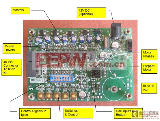
图2。马达控制子板外形图
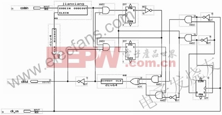
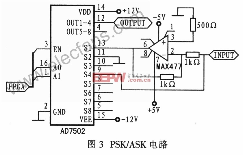
图3。步进马达控制逻辑方框图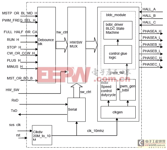
图4。BLDC马达控制逻辑方框图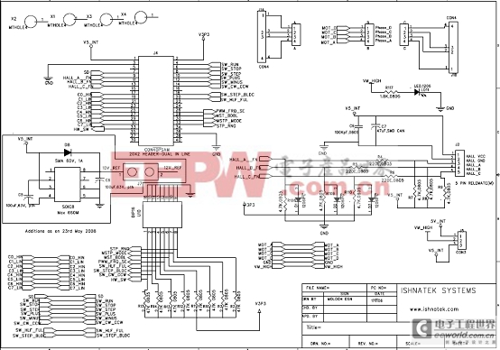
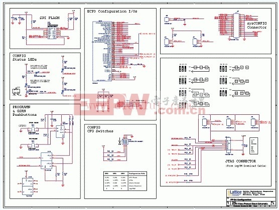
图5。马达控制子板电路图(1)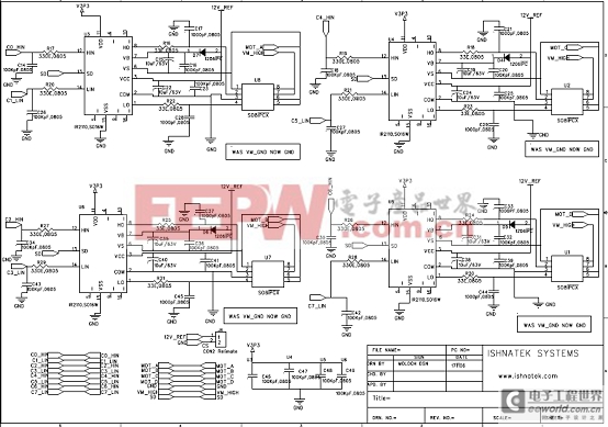
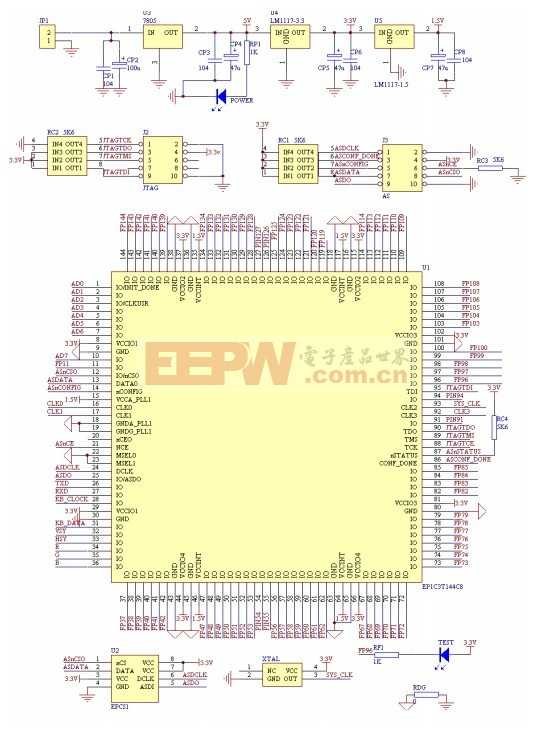
图6。马达控制子板电路图(2)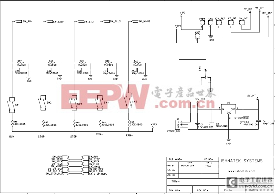
图7。马达控制子板电路图(3)
马达控制子板材料清单(BOM):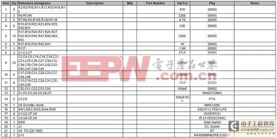


评论