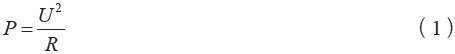
STC12C5A60S2系列双串口1T 8051单片机头文件
//--------------------------------------------------------------------------------
//新一代 1T 8051系列 单片机内核特殊功能寄存器 C51 Core SFRs
// 7 6 5 4 3 2 1 0 Reset Value
sfr ACC = 0xE0; //Accumulator 0000,0000
sfr B = 0xF0; //B Register 0000,0000
sfr PSW = 0xD0; //Program Status Word CY AC F0 RS1 RS0 OV F1 P 0000,0000
//-----------------------------------
sbit CY = PSW^7;
sbit AC = PSW^6;
sbit F0 = PSW^5;
sbit RS1 = PSW^4;
sbit RS0 = PSW^3;
sbit OV = PSW^2;
sbit P = PSW^0;
//-----------------------------------
sfr SP = 0x81; //Stack Pointer 0000,0111
sfr DPL = 0x82; //Data Pointer Low Byte 0000,0000
sfr DPH = 0x83; //Data Pointer High Byte 0000,0000
//--------------------------------------------------------------------------------
//新一代 1T 8051系列 单片机系统管理特殊功能寄存器
// 7 6 5 4 3 2 1 0 Reset Value
sfr PCON = 0x87; //Power Control SMOD SMOD0 LVDF POF GF1 GF0 PD IDL 0001,0000
// 7 6 5 4 3 2 1 0 Reset Value
sfr AUXR = 0x8E; //Auxiliary Register T0x12 T1x12 UART_M0x6 BRTR S2SMOD BRTx12 EXTRAM S1BRS 0000,0000
//-----------------------------------
sfr AUXR1 = 0xA2; //Auxiliary Register 1 - PCA_P4 SPI_P4 S2_P4 GF2 ADRJ - DPS 0000,0000
/*
PCA_P4:
0, 缺省PCA 在P1 口
1,PCA/PWM 从P1 口切换到P4 口: ECI 从P1.2 切换到P4.1 口,
PCA0/PWM0 从P1.3 切换到P4.2 口
PCA1/PWM1 从P1.4 切换到P4.3 口
SPI_P4:
0, 缺省SPI 在P1 口
1,SPI 从P1 口切换到P4 口: SPICLK 从P1.7 切换到P4.3 口
MISO 从P1.6 切换到P4.2 口
MOSI 从P1.5 切换到P4.1 口
SS 从P1.4 切换到P4.0 口
S2_P4:
0, 缺省UART2 在P1 口
1,UART2 从P1 口切换到P4 口: TxD2 从P1.3 切换到P4.3 口
RxD2 从P1.2 切换到P4.2 口
GF2: 通用标志位
ADRJ:
0, 10 位A/D 转换结果的高8 位放在ADC_RES 寄存器, 低2 位放在ADC_RESL 寄存器
1,10 位A/D 转换结果的最高2 位放在ADC_RES 寄存器的低2 位, 低8 位放在ADC_RESL 寄存器
DPS: 0, 使用缺省数据指针DPTR0
1,使用另一个数据指针DPTR1
*/
//-----------------------------------
sfr WAKE_CLKO = 0x8F; //附加的 SFR WAK1_CLKO
/*
7 6 5 4 3 2 1 0 Reset Value
PCAWAKEUP RXD_PIN_IE T1_PIN_IE T0_PIN_IE LVD_WAKE _ T1CLKO T0CLKO 0000,0000B
b7 - PCAWAKEUP : PCA 中断可唤醒 powerdown。
b6 - RXD_PIN_IE : 当 P3.0(RXD) 下降沿置位 RI 时可唤醒 powerdown(必须打开相应中断)。
b5 - T1_PIN_IE : 当 T1 脚下降沿置位 T1 中断标志时可唤醒 powerdown(必须打开相应中断)。
b4 - T0_PIN_IE : 当 T0 脚下降沿置位 T0 中断标志时可唤醒 powerdown(必须打开相应中断)。
b3 - LVD_WAKE : 当 CMPIN 脚低电平置位 LVD 中断标志时可唤醒 powerdown(必须打开相应中断)。
b2 -
b1 - T1CLKO : 允许 T1CKO(P3.5) 脚输出 T1 溢出脉冲,Fck1 = 1/2 T1 溢出率
b0 - T0CLKO : 允许 T0CKO(P3.4) 脚输出 T0 溢出脉冲,Fck0 = 1/2 T1 溢出率
*/
//-----------------------------------
sfr CLK_DIV = 0x97; //Clock Divder - - - - - CLKS2 CLKS1 CLKS0 xxxx,x000
//-----------------------------------
sfr BUS_SPEED = 0xA1; //Stretch register - - ALES1 ALES0 - RWS2 RWS1 RWS0 xx10,x011
/*
ALES1 and ALES0:
00 : The P0 address setup time and hold time to ALE negative edge is one clock cycle
01 : The P0 address setup time and hold time to ALE negative edge is two clock cycles.
10 : The P0 address setup time and hold time to ALE negative edge is three clock cycles. (default)
11 : The P0 address setup time and hold time to ALE negative edge is four clock cycles.
RWS2,RWS1,RWS0:
000 : The MOVX read/write pulse is 1 clock cycle.
001 : The MOVX read/write pulse is 2 clock cycles.
010 : The MOVX read/write pulse is 3 clock cycles.
011 : The MOVX read/write pulse is 4 clock cycles. (default)
100 : The MOVX read/write pulse is 5 clock cycles.
101 : The MOVX read/write pulse is 6 clock cycles.
110 : The MOVX read/write pulse is 7 clock cycles.
111 : The MOVX read/write pulse is 8 clock cycles.
*/
//--------------------------------------------------------------------------------
//新一代 1T 8051系列 单片机中断特殊功能寄存器
//有的中断控制、中断标志位散布在其它特殊功能寄存器中,这些位在位地址中定义
//其中有的位无位寻址能力,请参阅 新一代 1T 8051系列 单片机中文指南
// 7 6 5 4 3 2 1 0 Reset Value
sfr IE = 0xA8; //中断控制寄存器 EA ELVD EADC ES ET1 EX1 ET0 EX0 0x00,0000
//-----------------------
sbit EA = IE^7;
sbit ELVD = IE^6; //低压监测中断允许位
sbit EADC = IE^5; //ADC 中断允许位
sbit ES = IE^4;
sbit ET1 = IE^3;
sbit EX1 = IE^2;
sbit ET0 = IE^1;
sbit EX0 = IE^0;
//-----------------------
sfr IE2 = 0xAF; //Auxiliary Interrupt - - - - - - ESPI ES2 0000,0000B
//-----------------------
// 7 6 5 4 3 2 1 0 Reset Value
sfr IP = 0xB8; //中断优先级低位 PPCA PLVD PADC PS PT1 PX1 PT0 PX0 0000,0000
//--------
sbit PPCA = IP^7; //PCA 模块中断优先级
sbit PLVD = IP^6; //低压监测中断优先级
sbit PADC = IP^5; //ADC 中断优先级
sbit PS = IP^4;
sbit PT1 = IP^3;
sbit PX1 = IP^2;
sbit PT0 = IP^1;
sbit PX0 = IP^0;
//-----------------------
// 7 6 5 4 3 2 1 0 Reset Value
sfr IPH = 0xB7; //中断优先级高位 PPCAH PLVDH PADCH PSH PT1H PX1H PT0H PX0H 0000,0000
sfr IP2 = 0xB5; // - - - - - - PSPI PS2 xxxx,xx00
sfr IPH2 = 0xB6; // - - - - - - PSPIH PS2H xxxx,xx00
//-----------------------
//新一代 1T 8051系列 单片机I/O 口特殊功能寄存器
// 7 6 5 4 3 2 1 0 Reset Value
sfr P0 = 0x80; //8 bitPort0 P0.7 P0.6 P0.5 P0.4 P0.3 P0.2 P0.1 P0.0 1111,1111
sfr P0M0 = 0x94; // 0000,0000
sfr P0M1 = 0x93; // 0000,0000
sfr P1 = 0x90; //8 bitPort1 P1.7 P1.6 P1.5 P1.4 P1.3 P1.2 P1.1 P1.0 1111,1111
sfr P1M0 = 0x92; // 0000,0000
sfr P1M1 = 0x91; // 0000,0000
sfr P1ASF = 0x9D; //P1 analog special function
sfr P2 = 0xA0; //8 bitPort2 P2.7 P2.6 P2.5 P2.4 P2.3 P2.2 P2.1 P2.0 1111,1111
sfr P2M0 = 0x96; // 0000,0000
sfr P2M1 = 0x95; // 0000,0000
sfr P3 = 0xB0; //8 bitPort3 P3.7 P3.6 P3.5 P3.4 P3.3 P3.2 P3.1 P3.0 1111,1111
sfr P3M0 = 0xB2; // 0000,0000
sfr P3M1 = 0xB1; // 0000,0000
sfr P4 = 0xC0; //8 bitPort4 P4.7 P4.6 P4.5 P4.4 P4.3 P4.2 P4.1 P4.0 1111,1111
sfr P4M0 = 0xB4; // 0000,0000
sfr P4M1 = 0xB3; // 0000,0000
// 7 6 5 4 3 2 1 0 Reset Value
sfr P4SW = 0xBB; //Port-4 switch - LVD_P4.6 ALE_P4.5 NA_P4.4 - - - - x000,xxxx
sfr P5 = 0xC8; //8 bitPort5 - - - - P5.3 P5.2 P5.1 P5.0 xxxx,1111
sfr P5M0 = 0xCA; // 0000,0000
sfr P5M1 = 0xC9; // 0000,0000
//--------------------------------------------------------------------------------
//新一代 1T 8051系列 单片机定时器特殊功能寄存器

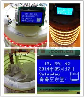

评论