基于ATmega128RFA1设计的低功耗ZigBee解决方
Atmel公司的ATmega128RFA1是低功耗CMOS 8位MCU,采用AVR增强性RISC架构和2.4GHz ISM频段高数据速率收发器,吞吐量达1 MIPS per MHz .无线收发器的数据速率从250 kb/s到高达2 Mb/s,还提供帧处理,有杰出的接收灵敏度(-100dBm)和高发送功率(达3.5dBm),主要应用在ZigBee® / IEEE 802.15.4-2006/2003,通用的2.4GHz ISM频段, F4CE, SP100, WirelessHART™, ISM和IPv6 / 6LoWPAN.本文介绍了ATmega128RFA1主要特性, 基本应用电路图和相应的材料清单(BOM),以及扩展特性应用电路图和评估板特性与电路图.
The ATmega128RFA1 is a low-power CMOS 8 bit microcontroller based on the AVR enhanced RISC architecture combined with a high data rate transceiver for the 2.4 GHz ISM band. It is derived from the ATmega1281 microcontroller and the AT86RF231 radio transceiver.
By executing powerful instructions in a single clock cycle, the device achieves throughputs approaching 1 MIPS per MHz allowing the system designer to optimize power consumption versus processing speed.
The radio transceiver provides high data rates from 250 kb/s up to 2 Mb/s, frame handling, outstanding receiver sensitivity and high transmit output power enabling a very robust wireless communication.
ATmega128RFA1主要特性:
• High Performance, Low Power AVR® 8-Bit Microcontroller
• Advanced RISC Architecture
- 135 Powerful Instructions – Most Single Clock Cycle Execution
- 32x8 General Purpose Working Registers
- Fully Static Operation
- Up to 16 MIPS Throughput at 16 MHz and 1.8V
- On-Chip 2-cycle Multiplier
• Non-volatile Program and Data Memories
- 128K Bytes of In-System Self-Programmable Flash
• Endurance: 2000 Write/Erase Cycles @ 85℃
- 4K Bytes EEPROM
• Endurance: 2000 Write/Erase Cycles @ 85℃
- 16K Bytes Internal SRAM
• JTAG (IEEE std. 1149.1 compliant) Interface
- Boundary-scan Capabilities According to the JTAG Standard
- Extensive On-chip Debug Support
- Programming of Flash EEPROM, Fuses and Lock Bits through the JTAG interface
• Peripheral Features
- Multiple Timer/Counter PWM channels
- Real Time Counter with Separate Oscillator
- 10-bit, 330 ks/s A/D Converter; Analog Comparator; On-chip Temperature Sensor
- Master/Slave SPI Serial Interface
- Two Programmable Serial USART
- Byte Oriented 2-wire Serial Interface
• Advanced Interrupt Handler
• Watchdog Timer with Separate On-Chip Oscillator
• Power-on Reset and Low Current Brown-Out Detector
• Advanced Power Save Modes
• Fully integrated Low Power Transceiver for 2.4 GHz ISM Band
- Supported Data Rates: 250 kb/s and 500 kb/s, 1 Mb/s, 2 Mb/s
- -100 dBm RX Sensitivity; TX Output Power up to 3.5 dBm
- Hardware Assisted MAC (Auto-Acknowledge, Auto-Retry)
- 32 Bit IEEE 802.15.4 Symbol Counter
- Baseband Signal Processing
- SFR-Detection, Spreading; De-Spreading; Framing ; CRC-16 Computation
- Antenna Diversity and TX/RX control
- TX/RX 128 Byte Frame Buffer
• Hardware Security (AES, True Random Generator)
• Integrated Crystal Oscillators (32.768 kHz 16 MHz)
• I/O and Package
- 38 Programmable I/O Lines
- 64-pad QFN (RoHS/Fully Green)
• Temperature Range: -40℃ to 85℃ Industrial
• Supply voltage range 1.8V to 3.6V with integrated voltage regulators
• Ultra Low Power consumption (1.8 to 3.6V) for Rx/Tx AVR: 18.6 mA
- CPU Active Mode (16MHz): 4.1 mA
- 2.4GHz Transceiver: RX_ON 12.5 mA / TX 14.5 mA (maximum TX output power)
- Deep Sleep Mode: 250nA @ 25℃
• Speed Grade: 0 – 16 MHz @ 1.8 – 3.6V
ATmega128RFA1应用:
• ZigBee®/IEEE 802.15.4-2006/2003™– Full And Reduced Function Device (FFD/RFD)
• General Purpose 2.4GHz ISM Band Transceiver with Microcontroller
• RF4CE, SP100, WirelessHART™, ISM Applications and IPv6 / 6LoWPAN
图1.ATmega128RFA1方框图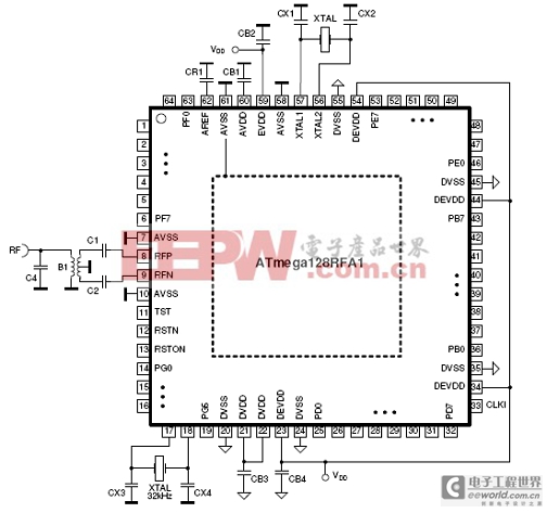
图2.ATmega128RFA1基本应用电路图
图2基本应用电路图材料清单(BOM):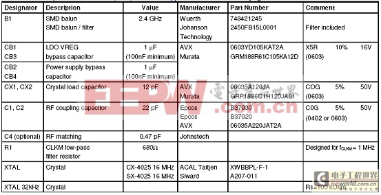

图3.ATmega128RFA1扩展特性应用电路图
ATmega128RFA1评估板
The ATmega128RFA1 evaluation kit enables development, debugging and demonstration of IEEE 802.15.4 compliant wireless applications such as ZigBee and 6LoWPAN. The kit contains two evaluation boards for the ATmega128RFA1 device, covering the 2.4GHz ISM bands for use with STK600.
图4.ATmega128RFA1评估板外形图
图5.ATmega128RFA1评估板电路图


评论