模拟集成电路的低电压系统-Analog ICs for Lo
Voltage Regulation
General Information About Voltage Regulators
Maxim has scores of regulators that generate low voltage or convert low voltages to other levels. They include low-dropout linear regulators, switched-capacitor charge-pump converters, and inductor-based switching regulators.Low dropout linear regulators (LDOs) are simple to use, require an input voltage greater than the output, and regulate up to 4A of output current. LDOs are less noisy and less expensive than switching regulators, but they dissipate more power (and generate more heat) as the applied input voltage rises. Linear regulators can, however, be quite efficient for applications with a low input-to-output voltage differential (efficiency is proportional to VOUT/VIN).
Charge-pump converters can boost a DC voltage to a higher value, or produce a voltage of opposite polarity from the input voltage. They use capacitors for energy storage and provide small, low-cost, DC-DC conversion circuits. However, they are limited in output current to less than 0.75A, and so they are restricted to low-power applications.
Inductor-based switching regulators offer both low- and high-power DC-DC voltage conversion, and can either step up (boost) or step down (buck) an input voltage. Maxim's boost regulators offer up to 4A of output current, and our buck regulators offer up to 60A of output current.
Low-Dropout Linear Regulators
Linear regulators require that the input voltage is greater than the output voltage. The minimum required difference between the input voltage and the output voltage is called the dropout voltage. Modern linear regulators have dropout voltages much lower than those of early linear regulators, like the LM7905, and have come to be called low-dropout regulators, or LDOs. Maxim offers a wide variety of LDOs with preset positive output voltages as low as 0.75V and adjustable voltages down to 0.5V. We also offer negative LDOs with outputs from -2.5V to -5V.LDOs make regulating to a low DC voltage easy and economical. The MAX1589 LDO family is simple to use, feature preset output voltages that vary from 0.75V to 3.0V, and operate with less than 0.175V of dropout at their full 500mA of output current. The MAX1818 LDO family also offers preset output voltages from 0.75V to 3.0V, 500mA of output current, and feature adjustable output voltage down to 1.25V and a dropout voltage of only 0.12V at their full 500mA of output current.
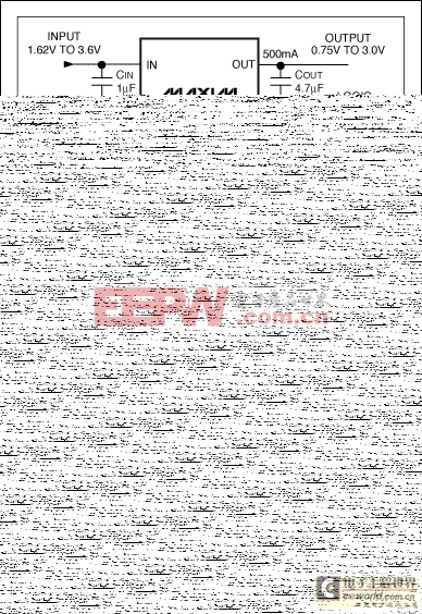
Figure 1. The MAX1589 500mA LDO has preset outputs of 0.75V, 1.0V, 1.3V, 1.5V, 2.5V, and 3.0V. The MAX1818 500mA LDO has preset outputs of 1.5V, 1.8V, 2.0V, 2.5V, 3.0V, and 5.0V or an adjustable output from 1.25V to 5V.
The MAX8510 LDO series incorporates several features important in the design of portable equipment: small size (SC70), low dropout voltage (120mV at 120mA), and low supply current (90µA max.). The MAX8510/MAX8511 are preset to a variety of output voltages between 1.5V and 4.5V, while the MAX8512's output voltage can be adjusted with an external divider.
Charge-Pump Voltage Converters
For low-current applications, the simplest solution for boosting 3V to 5V is a capacitor-based regulating charge pump (Figure 2). The industry-standard 7660 and most other charge pumps don't regulate VOUT, but the MAX619 includes an analog reference and error amplifier whose output controls a set of internal switches connected to external capacitors. The switch-capacitor network can double or triple VIN, and the MAX619 regulates by switching between these modes of operation. As indicated, this circuit produces 20mA at 5V ±4% for inputs that range between 2V and 3.6V. For inputs between 3.0V and 3.6V, the output-current capability is 50mA.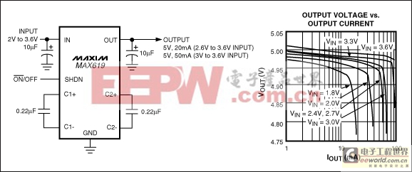
Figure 2. Occupying less than 0.1in² of board space, the MAX619 regulated charge-pump converter generates 20mA at 5V ±4% for inputs of 2V to 3.6V and 50mA from 3V to 3.6V.
The MAX5008 regulated 5V USB charge pump provides an output current of up to 125mA with supply voltages down to 2.9V, and is suitable for USB host devices with 3.0V or 3.3V supplies.
Systems that handle bipolar signals usually require a negative supply, which can be generated locally if necessary. A simple solution is to use a charge-pump inverter such as the MAX889.
Inductor-Based, Switch-Mode Regulators
Switching regulators provide single or multiple outputs. Depending on the output power level, these devices are controlled by pulse-frequency modulation (PFM), pulse-width modulation (PWM), or both.. PFM control schemes, which allow high efficiency with light loads, permit the regulator to operate with quiescent supply currents as low as 10µA. PWM schemes consume more power, but they allow fixed-frequency operation for better control of noise and EMI. Some converters switch between the two control schemes based on a control signal or the load-current level.While LDOs are efficient for low values of (VIN - VOUT), many applications have an input voltage that is significantly higher than the output voltage. In this case, efficiency dictates the use of a buck-switching regulator. RF applications such as radios and cellular phones can easily use switching regulators, but care must be taken to avoid introducing noise at the sensitive IF frequencies.
An ideal choice for RF applications is the MAX1684 switching regulator. This device delivers 1A at 3.3V from inputs of 4V to 12V with efficiencies up to 97%, has a 300kHz internal oscillator, and features internal MOSFETs for ease of use.
An efficient buck regulator is also a good choice for upgrading an existing logic board to accommodate lower-voltage, lower-power ICs. These boards typically have 3.3V available, but they require a 1.8V supply for the new low-voltage logic. A linear regulator can easily convert 3.3V to 1.8V, but the power dissipation is prohibitive for higher load currents. At 2A, for instance, the linear regulator would dissipate 3W and require a heat-sink. The MAX1830 high-efficiency switcher (Figure 3), however, delivers 20mA to 2A with efficiencies exceeding 90% and requires no external MOSFETs, thus eliminating the need for a heat-sink.
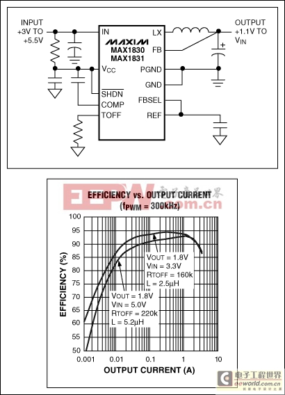
Figure 3. The MAX1830 switching regulator converts 3.3V to 1.8V with efficiency greater than 90% from 20mA to 2A, and requires no external MOSFETs.
The MAX1830 comes in a very small, 16-pin QSOP package and has an input range of 3V to 5.5V. Its quiescent operating current drops from 325µA to only 0.2µA in standby mode. High switching frequency (up to 1MHz) allows the device to operate with small, low-cost, surface-mount components.
Multi-output switching regulators are intended for systems designed to operate with multiple supplies. Applications such as the generation of VCC voltages in a notebook computer, for example, are well served by the MAX1999, which generates four regulated supply voltages (Figure 4).
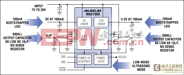
Figure 4. The MAX1999 switching regulator generates four output voltages and has two high-efficiency, high-power switch-mode regulators and two low-power linear regulators. It also includes a power-good output, shutdown control, current limiting, and pin-programmable power-up sequencing.
Data Converters

DIY机械键盘相关社区:机械键盘DIY


评论