电流型测试仪表放大器提升压电加速度计性能
电路抑制由压电传感器及其电缆产生的容性耦合噪声。
本文引用地址:http://www.eepw.com.cn/article/193492.htm一个典型的压电传感器由表面上金属化电极的PZT-5A陶瓷材料组成。在电极处使用导电环氧将传感器连接到外部电缆。绝缘胶粘合装置元件到待测结构上,使传感器与接地参考电位隔离。压电片面向预期加速度的方向。当安放在目标结构上时,压电片成为简单的压力传感器和加速度计,产生正比于压力且平行于压电片极化方向的电压。压电片容性阻抗在低频时呈现很大的电抗,使压电片和电缆易受周围电气设备和电源线的干扰。传感器远距离安放时,需要使用屏蔽的互连电缆,但即使屏蔽,对去除共模信号也不是完全有效,因为压电片的导电表面仍会获取噪声。
提取传感器信号的一个方法是使用仪表放大器,它只放大传感器所产生的电位。放大器抑制出现在传感器各端的共模耦合噪声电位。
典型的微型压电片传感器直径0.125英寸,0.0075英寸厚,相当于几乎500 pF的电容。如果测量应用需要限制激励频率在10Hz或更低的动态响应,传感器输出电抗可达到10几MΩ的范围。电路印制板的绝缘层和周围湿度使放大器输入阻抗有几乎10 MΩ的实际限制。
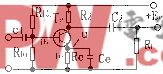
必须谨慎选择绝缘方法和使用保护电位,必须使用输入偏置电流为微微安级的放大器。否则,传感器电容和放大器的输入偏置电流电阻,对仪表放大器的信号施加相位偏移。为消除保护和复杂的绝缘需要,图1电路使用带反馈的仪表放大器,测量传感器短路电流,而不是开路电压。传感器和信号地之间的共模电压VCM来自周围杂散电容耦合带来的噪声源。下面的公式描述了传感器输出电流i和其开路输出电压ES的关系:
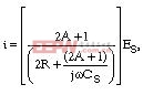
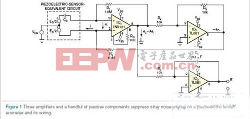
图1中,A代表IC1的电压增益,R=R1=R2。电阻R1和R2为IC1(INA121仪表放大器)提供反馈和输入偏置电流回路,电阻RG设置放大器增益。INA121的输入偏置电流为0.5pA,在10MΩ反馈电阻上产生5µV电压偏置。放大器增益为500倍时,IC1输出偏置达到2.5 mV。放大器IC2 TL081提供单位增益的信号极性变换。
如果2A+1>>2RjωCS,则i≈jωCSES。放大器IC1输入电压V1变为零,因为放大器输入终端通过传感器起虚短电路的作用。取仪表放大器和反相放大器输出、两个反馈电阻和仪表放大器输入端子构成回路的电压和(其电位差为零),得到eO=jωRCES,其中eO表示IC1的输出,也是IC2输出的负值。
在下面的公式中,用运算放大器做的积分器IC3给出在IC3输出的ES。

图1中的元器件值,IC1提供500倍增益。电阻R1和R2为10 MΩ,压电传感器的电容为500 pF。对最高频率10Hz,量值为2RωCS=0.62A+1=501和传感器输出ES,也没有相位误差E'。电路能测量准静态压力的改变;电路能维持C1上的电荷,从而对电路频率响应构成限制。
英文原文:
Circuit suppresses capacitively coupled noise pickup by piezoelectric sensor and its wiring.
Dave Wuchinich, Modal Mechanics, Yonkers, NY; Edited by Brad Thompson and Fran Granville -- EDN, 11/23/2006
A typical piezoelectric sensor comprises a disk of PZT-5A ceramic material with metallized electrodes on its
surfaces. Applying electrically conductive epoxy to the electrodes connects external wiring to the sensor. An insulating adhesive attaches the assembly to the structure under test and isolates the sensor from ground-referenced potentials. The disk faces the direction of the expected acceleration. When you mount the piezoelectric disk on a target structure, it serves as a simple force sensor and accelerometer by producing a voltage that's directly proportional to the force acting parallel to the disk's direction of polarization. A piezoelectric disk's capacitive impedance presents a large reactance at low frequencies, making the disk and its wiring susceptible to interference that surrounding electrical equipment and power lines produce. Placing the sensor in a remote location requires shielded interconnecting cable, but even shielding is not entirely effective in removing common-mode signals because noise pickup can still occur at the disk's conductive surfaces.
.
One method of extracting the sensor's signal employs an instrumentation amplifier, which amplifies only the potential the sensor produces; the amplifier rejects common-mode-coupled noise potential that appears on each of the sensor's terminals.
A typical miniature piezoelectric- disk sensor that's 0.125 in. in diameter and 0.0075 in. thick presents a capacitance of approximately 500 pF. If the measurement application requires a dynamic response to force excitation frequencies of 10 Hz or below, the sensor's output reactance ranges into the tens of megohms. The circuit's pc-board insulating substrate and ambient humidity impose a practical limit of approximately 10 MΩ on the amplifier's input resistance.
You must carefully choose insulation and apply guarding potentials, and you must use an amplifier with picoampere input-bias currents. Otherwise, the sensor's capacitance and the amplifier's input-bias-current resistors impose a phase shift on the signal you apply to the instrumentation amplifier. To eliminate guarding and elaborate insulation requirements, the circuit in Figure 1 uses an instrumentation amplifier with feedback to measure the sensor's short-circuit current and not its open-circuit voltage. VCM, the common-mode voltage between the sensor and the signal ground, results from nearby noise sources resulting from stray capacitive coupling. The following equation relates the sensor's output current, i, and its open-circuit output voltage, ES:
where A represents IC1's voltage gain, and R=R1=R2 in Figure 1. Resistors R1 and R2 provide feedback and input-bias-current-return paths for IC1, an INA121 instrumentation amplifier, and resistor RG sets the amplifier's gain. The INA121's input-bias-offset current of 0.5 pA produces 5 µV of voltage offset across its 10-MΩ feedback resistors. At an amplifier gain of 500, IC1's output offset amounts to 2.5 mV. Amplifier IC2, a TL081, provides unity-gain signal inversion.
If 2A+1>>2R
jωCS, then i≈jωCSES, and amplifier IC1's input voltage, VI, vanishes because the amplifier's input terminals act as a virtual short circuit across the sensor. Taking the sum of voltages around the loop comprising the instrumentation and inverting amplifiers' output, the two feedback resistors and the instrumentation amplifier's input terminals, whose potential difference is zero, yields eO=jωRCES, where eO represents IC1's output and also the negative value of IC2's output.
An operational-amplifier-based integrator, IC3, delivers the value for ES at IC3's output, E' in the following equation.
For the component values in Figure 1, IC1 provides a gain of 500. Resistors R1 and R2 are equal at 10 MΩ, and the piezoelectric sensor's capacitance measures 500 pF. For the highest frequency of interest, 10 Hz, the quantity 2RωCS=0.62A+1=501 and the sensor's output, ES, appear without phase error as E'. This circuit can measure quasistatic force changes; the circuit's ability to sustain a charge on C1 imposes the ultimate limit on the circuit's frequency response.
加速度计相关文章:加速度计原理


评论