Altera Cyclone IV GX系列FPGA开发方案
Alterareg; Cyclonereg; IV GX FPGA开发套件为迅速开始开发低成本、低功耗FPGA系统级设计提供了全面的、同类最佳的设计环境。该套件帮助您缩短了产品开发周期,使您能够更迅速的将产品推向市场,树立新的产品里程碑。采用这一平台,您能够:
使用Cyclone IV GX PCI Express硬核知识产权(IP)和PCI-SIGreg;兼容电路板,开发并测试PCI Expressreg; Gen1 x1、x2、x4端点设计。
使用板上DDR2存储器,通过其扩展功能,高速中间链接卡(HSMC)连接器,开发并测试多通路协议桥接设计。Altera合作伙伴提供30多种不同的HSMC,以及CPRI、SATA和SDI等支持协议。
重新使用套件电路板测试系统提供的实例设计,加速您的FPGA设计。
针对您产品的低成本和低功耗电路板,使用套件的主板作为设计模型。
Cyclone IV GX FPGA开发套件包括:
Cyclone IV GX FPGA开发板(参见图1)
安装的器件
F896封装的Cyclone IV GX EP4CGX150N FPGA
配置状态和设置单元
通过MAXreg; II EPM2210 CPLD和闪存进行被动串行(PS)配置
使用Quartusreg;II编程器的板上USB-BlasterTM下载电缆
时钟
板上时钟振荡器:50 MHz、100 MHz(可设置)和125 MHz
用于外部时钟输入的SMA连接器
用于时钟输出的SMA连接器
通用用户输入和输出
LED
LCD显示屏
按键和双列直插封装(DIP)开关
存储器件
128-MB DDR2 SDRAM,支持32位数据总线。
64-MB同步闪存和4-MB SSRAM
元件和接口
PCI Express边沿连接器
10/100/1000-Mbps以太网PHY,提供RJ-45连接器。
两个HSMC连接器
电源测量电路
电源
笔记本计算机直流输入
PCI Express边沿连接器电源
其他特性
PCI Express短卡
符合RoHS
Cyclone IV GX FPGA开发套件软件组成(可以通过表2下载)
设计实例
电路板更新入口,含有Niosreg;II处理器网络服务器,支持远程系统更新。
电路板测试系统
完整的文档(参见表2)
免费的Quartus II网络版软件,包括对Cyclone IV FPGA的支持,以及:
Nios II嵌入式设计套装
MegaCorereg;IP库包括PCI Express、三速以太网、SDI和DDR2高性能控制器MegaCore IP内核
通过OpenCore Plus进行IP评估
回环和调试HSMC
电源适配器和电缆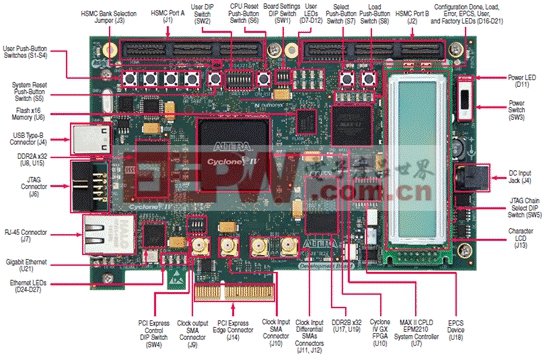
图2.Cyclone IV GX FPGA开发套件外形图和主要元件分布图
The board features the following major component blocks:
■ Cyclone IV GX EP4CGX150DF31 FPGA in the 896-pin FineLine BGA (FBGA)package
■ 1.2-V core power
■ MAXreg; II EPM2210GF256 CPLD in the 256-pin FBGA package
■ 1.8-V core power
■ FPGA configuration circuitry
■ MAX II CPLD EPM2210 System Controller and flash fast passive parallel (FPP) configuration
■ Active serial configuration
■ On-board USB-BlasterTM for use with the Quartusreg; II Programmer
■ JTAG header for external USB-Blaster with the Quartus II Programmer
■ On-Board ports
■ Embedded USB-Blaster
■ One gigabit Ethernet port
■ Communication ports
■ PCI Express (PCIe) edge connector
■ 10/100/1000BASE-T Ethernet PHY with RJ-45 connector
■ Two High-Speed Mezzanine Card (HSMC) interfaces
■ On-Board memory
■ 4-MB (x16) Synchronous Static Random Access Memory (SSRAM)
■ Two 32-MB (x32) DDR2 SDRAM
■ 64-MB flash
■ On-Board clocking circuitry
■ 50.000-MHz oscillator
■ 125.000-MHz oscillator
■ SMA clock input
■ SMA clock output
■ Programmable oscillator (default: 100.000-MHz)
■ General user I/O
■ LEDs and display
■ Eight FPGA user LEDs
■ One configuration done LED
■ One error LED
■ Five Ethernet status LEDs
■ One USB status LED
■ One power status LED
■ Five configuration LEDs
■ A two-line 16-character LCD display
■ Push-Button switches
■ One CPU reset push-button switch
■ One MAX II configuration reset push-button switch
■ One program-load push-button switch—configure the FPGA from flash memory
■ One program-select push-button switch—select image to load from flash memory or serial configuration (EPCS) device
■ Four general user push-button switches
■ DIP switches
■ Board settings DIP switch
■ JTAG chain select DIP switch
■ PCIe control DIP switch
■ Configuration settings DIP switch
■ User DIP switch
■ Power supply
■ 16-V DC input
■ 2.5-mm barrel jack for DC power input
■ On/Off slide power switch
■ On-Board power measurement circuitry
■ 20-W per HSMC interface
■ Mechanical
■ PCIe small form factor board
■ Bench-top operation


评论