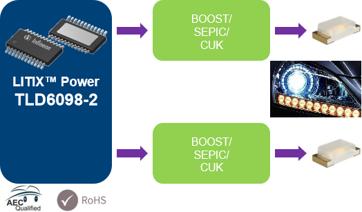
Boost driver for long LED strings
Figure 10. Inductor temperature rise. The calculator is available from Coilcraft®.
本文引用地址:http://www.eepw.com.cn/article/188142.htm
Circuit description
Overview
This reference design is for a high-voltage, boost current source for very long strings of LEDs. Applications include LCD TV backlighting, LCD monitor backlighting, streetlights, and parking garage lights. Long LED strings can be a very cost-effective way to drive LEDs. Also, since the LEDs will have exactly the same current, brightness variations are nicely controlled. This design has a 24V input, up to an 80V LED output, and drives 350mA through the LED string. The measured input power is 29.3W and the output power is 26.4W for about 90% efficiency.
PCB
The printed circuit board (PCB) is a general-purpose board for MAX16834 boost designs (Figures 1 and 3). Therefore, there are many components that are either shorted or not populated. These components are indicated on the schematic (Figure 2). Figure 4 shows a bill of materials for this design.
Topology
This design is for a 300kHz discontinuous-boost regulator. In Figure 5, the spreadsheet printout shows the calculated RMS and peak currents in the MOSFET and inductor. Discontinuous designs do, admittedly, have some disadvantages, notably higher MOSFET and inductor currents. However, since the output current is essentially zero when the MOSFET (Q1) turns on, the reverse recovery losses in the output diode (D2) are minimal. This advantage outweighs the design disadvantages, because overheating and noise caused by reverse-recovery currents are difficult to manage. Inspecting the circuit waveforms in Figure 6, you see that the on-time of the MOSFET is about 1.6µs. Once the MOSFET turns off, the drain voltage jumps to 75V for about 1µs, while the inductor conducts to the output capacitors. After that, the inductor energy is essentially drained, and for another microsecond the inductance and MOSFET output capacitance ring until the next on-time.
MOSFET drive
Because of the discontinuous design, the peak MOSFET currents are more than twice what they would be with a continuous design. However, since there is no current through the MOSFET during turn-on, it only experiences switching losses during turn-off. The MAX16834 drives the MOSFET hard enough for the switch to turn off in about 20ns (Figure 7), thereby keeping the temperature rise low. If EMI becomes a problem, the series resistance and diode on the MOSFET gate can be altered to adjust the switching times. If needed, place a second MOSFET, Q2, parallel to Q1 to reduce the temperature rise.
Output capacitance
For the input and output capacitance, the driver uses long-life electrolytic capacitors. Electrolytic capacitors are neither as durable nor as small as ceramic capacitors, but they have the advantage of providing plenty of capacitance at an economical price. To maintain a low profile (10mm), the capacitors lie in a horizontal orientation. The input and output capacitors are rated for 4000 hours and 8000 hours, respectively, at a temperature of +105°C. As a general rule, electrolytic capacitors double their lifetimes for every 10°C reduction of ambient temperature. This means that for an ambient of +65°C, you can expect the input/output capacitors to maintain performance for 64kWh/128kWh. In Figure 5 the spreadsheet printout indicates that, to achieve the desired output-ripple voltage, you need only about 6µF of output capacitance. Because electrolytic capacitors have a limited ripple-current capability, this design uses two 47µF capacitors. The large amount of capacitance eliminates most of the switching-frequency ripple voltage (Figure 8). However since the capacitance is electrolytic with significant equivalent series inductance (ESL), the circuit noise created when the switching MOSFET turns off is not fully filtered. Adding ceramic capacitance or a low-Q LC filter on the output reduces this problem. Since each of these options has some cost, it is best to determine whether there is a problem with the high-frequency spike before trying to fix it.
Dimming
The MAX16834 is well suited for dimming. When PWMDIM (pin 10 of the IC) goes low, three things happen. First, the gate drive (pin 13) of the switching MOSFET, Q1, goes low. This prevents additional energy from being delivered to the LED string. Second, the gate drive (pin 18) of the dimming MOSFET, Q3, goes low. In addition to immediately curtailing the LED string current, the dimming MOSFET holds the voltage on the output capacitors constant during the off-time. Finally, to keep the compensation capacitance frozen at a steady-state voltage, the COMP (pin 3) goes to high impedance. The high impedance of the COMP pin ensures that the IC will start at the correct duty cycle immediately after PWMDIM returns high. Each of these actions, plus the fact that in a discontinuous design the inductor starts at zero current for every cycle, allows for very short PWM on-times, and thus, high dimming ratios. The only practical limitation to the dimming ratio is the frequency of the main switching driver. Since this design is for 300kHz, the smallest PWM on-time is about 3.33µs, which implies a dimming ratio up to 1500:1 (at a 200Hz dimming frequency). Figure 9 shows the current through the LED string with an on-time of less than 4µs. The LED string current is well behaved and provides the full 350mA during the pulse.
OVP
If the LED string were to open, the overvoltage protection (OVP) circuitry of the MAX16834 shuts down the driver for about 400ms between retry attempts. This design sets the OVP trip threshold to 101V.
MAX16834 pdf datasheet:http://www.elecfans.com/soft/39/2008/200808187352.html
FAULT#
The MAX16834 provides an output signal called FAULT#. This signal goes low whenever any internal fault (overcurrent or overvoltage) is detected. Once the fault is removed, FAULT# returns high. FAULT# is not latching.
Temperature rise
Due to the high efficiency of the circuit (~90%), the components of the driver remain cool. The obvious exception is the inductor, which has a +49°C rise that is higher than the Coilcraft predictor in Figure 10 (+27°C rise). The predictor looses accuracy when the peak currents exceed twice the RMS currents, which happens in discontinuous designs. For applications with high ambient temperatures, it may be necessary to use an automotive-rated inductor (+125°C) or use two 6µH inductors in series. For many applications with lower ambient temperatures, the single 12µH inductor would be acceptable.
Temperature measurements
The following temperatures were measured using actual LED loads:
| VIN: | 24VDC | |
| Ambient: | +22°C | ΔT |
| L1: | +71°C | 49°C |
| D2: | +43°C | 21°C |
| Q2: | +38°C | 16°C |
| Q3: | +34°C | 12°C |
Power-up procedure
- Attach a string of up to 23 LEDs between the LED+ post and LED- post.
- Attach a 24V, 2A power supply between the VIN post and GND post.
- If dimming is desired, attach a PWM signal (0 to 5V) to the DIM IN post and GND post.
- Turn on the 24V power supply.
- Adjust the PWM duty cycle, as desired, to obtain dimming.


评论