Use thermal analysis to predict an IC‘s transient behavior and avoid overheating
Figure 5. The forward voltage for a diode biased at constant current varies with temperature.
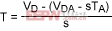
In Figure 5, TA is the ambient temperature and VDA is the diode voltage at ambient temperature. We, therefore, know one point on the graph and its slope. Slope can be derived by measuring the diode voltage at different temperatures in a temperature-controlled oven. Alternatively, you can use a number like 2mV/K, which is valid with minimal error for a wide range of diode currents.4 These numbers should apply to any other chip as well, but for accuracy it is always better to measure the slope associated with the current intended for biasing the diode. Any temperature can now be represented in terms of the diode voltage: 本文引用地址:http://www.eepw.com.cn/article/163233.htm
(Eq. 27)
Where:
T is the temperature for which the diode voltage is VD.
s is the slope of the graph (s 0).
Substituting this expression in Equations 11 and 12 yields the following:
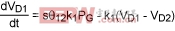
VD = sθJAP + VDA + (VDi - sθJAP - VDA)e-kAt (Eq. 28) VD = VDA + sθJAP(1 - e-kAt) (Eq. 29)
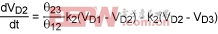
Substituting in Equations 18, 19, and 20 also yields:
(Eq. 30)
(Eq. 31)
(Eq. 32)
To apply our RC network properly for curve fitting the measured voltage-transient data for the diode, now we only need to set the magnitude of the current source as:
lS = sPG (Eq. 33)
Because s 0, you can realize Equation 33 by reversing the current source direction and setting its magnitude to |sPG|.
Experimental determination and verification of the RC network
We can demonstrate a practical application of the RC simulation model using the equations derived above and a linear LED driver like the MAX16828/MAX16815. These chips operate up to 40V using few external components, and the MAX16828 supplies an LED string with up to 200mA (Figure 6). The MAX16815 is pin-compatible with the MAX16828 and similar in function, but maximum output current is 100mA instead of 200mA.
Figure 6. Typical application circuit for the MAX16815/MAX16828 HBLED drivers.
Both LED drivers are suitable in automotive applications such as side lighting, automotive exterior rear combination lights, backlighting, and indicators. The MAX16828 can dissipate considerable heat if the internal MOSFET sees high current combined with a large dropout voltage. (The MOSFET does this when the LED string's forward voltage is low.) The voltage across RSENSE is regulated to 200mV ±3.5%, which allows that resistor to set the LED current. The chip's DIM input provides a wide range of PWM dimming for the LEDs and, because it also withstands high voltages, it can connect directly to the IN pin.
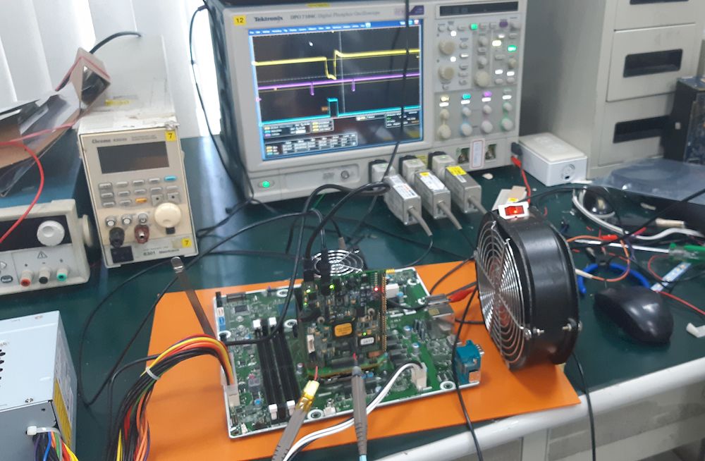
To obtain a direct indication of the die temperature, we measure the forward-bias voltage of an internal ESD diode connected between the DIM and IN pins. This diode is biased at ~100µA, causing its forward voltage to vary 2mV/K. (This can be confirmed by heating the part in a temperature-controlled oven.) Figure 7 shows the setup for these experiments. The 5V source and 56kΩ resistor provide 100µA for forward biasing the ESD diode. The driver is programmed to deliver 200mA of output current for the LEDs.
Figure 7. The test setup shown lets you measure transient die temperatures using an on-chip ESD diode. *EP indicates an exposed pad.
In this state the part carries a lot of current and our ESD diode measurement is in the path of that measurement. Consequently, we will get some error due to the parasitic resistance of the bond wire and internal metallization. From the internal layout and calculation of the length of bond wire, the worst-case parasitic resistance is estimated to be 50mΩ. With 200mA, this parasitic resistance will cause an error of around ±10mV (max) in our diode reading. Our accuracy error will be larger than ±5°C. Additionally, the ESD diode on the die is placed adjacent to the on-chip power MOSFET device and thermal-shutdown circuitry. This configuration makes the diode the best indicator of that region's temperature.
System definition 1
This next section describes how you can use a test setup to capture transient-thermal diode voltages for use in the system-definition equations presented above in Equations 7 and 21.
To calculate kA and θJA (for substitution in Equation 11), we heat the chip using a hot-air gun. The chip should be powered off because we do not want to generate internal heat. Heating the part with a hot-air gun causes the temperature of the package and die to rise together. You can monitor the die's temperature change by measuring the diode voltage on a scope (Figure 8).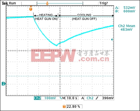
Figure 8. This diode-voltage transient includes exponential curves that represent heating with an external heat gun (falling curve) and cooling by removal of the heat gun (rising curve).
When the chip is heated, the diode voltage decreases with an exponential rate of change as the equation predicts. Near the center of the curve the hot-air gun is switched off, causing the package and die to begin cooling. The diode voltage rises, again following an exponential curve.
We do not know exactly how much heat is imparted from the heat gun to the chip. Therefore, to eliminate that unknown we first adjust Equation 28 to fit only the rising (cooling) part of the curve (Figure 8). This curve-fitting exercise lets us estimate the best value for kA. With no heat power transferred to the package during cooling, the package is simply cooling down with P = 0. Equation 28, therefore, simplifies t
VDB = VDA + (VDi - VDA)e-kAt (Eq. 34)
We know the values for VDA (643mV from the initial measurement at room temperature) and VDi (the reading for t = 0 reference). To determine kA, we must just adjust the equation so that it includes a couple of readings on the rising curve. This exercise yields kA = -0.0175. A graph of the readings (diode voltages in mV, with respect to time in seconds) and Equation 34 with the above kA is shown in Figure 9.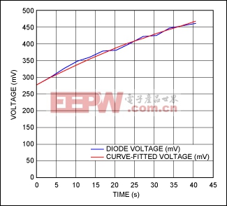
Figure 9. Equation 34, fitted to a couple of diode-voltage measurements, closely tracks all the diode measurements for a chip that is cooling after being heated with a heat gun.
As we can see in Figure 9, Equation 34 closely follows the measured data for kA = -0.0175. To verify that our equations are correct, we try to fit the falling curve on Equation 28 with the value determined for kA. The equation fits very accurately (Figure 10). Thus, we see that Equation 34 for the system discussed in System definition 1 closely matches the experimental data.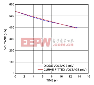
Figure 10. The curve-fitted Equation 28 closely tracks diode-voltage measurements for the falling (heating) portion of the curve.
System definition 2
Verification of the system 2 Equations 30, 31, and 32 is more difficult. We must generate heat on the die, measure the die temperature using the diode forward voltage, and fit that temperature value to a simulated value for the C1 voltage of the proposed RC network. This task is accomplished by writing a program using MATLAB.
It is important to record the thermal transient at a time for which the initial temperature of the whole chip is known. In that way we also know the initial capacitor voltages for solving the RC network. Using the same test setup (see Figure 7), we now turn on the current and capture the diode voltage on a scope (Figure 11).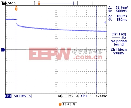
Figure 11. A forward-voltage transient from the MAX16828's internal diode signals that an on-board MOSFET has turned on and is generating heat.
Similar transients are recorded for three different power-dissipation levels, and one curve is fitted to that data. The circuit in Figure 12 is the result of fitting from the first set of data in which the power dissipation is 1.626W. The graph in Figure 13 compares the measured and fitted data. Similarly, the graph in Figure 14 shows how the RC network fits the second set of readings (power dissipation of 2.02W). The graph in Figure 15 shows how it fits the third set of readings (power dissipation of 1.223W).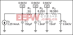
Figure 12. With component values as shown, this RC network models the chip's thermal transient when heat is generated on the die.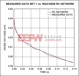
Figure 13. Measured vs. curve-fitted results for the chip's heating curve when the die is dissipating 1.626W.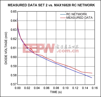
Figure 14. Measured vs. curve-fitted results for the chip's heating curve when the die is dissipating 2.02W.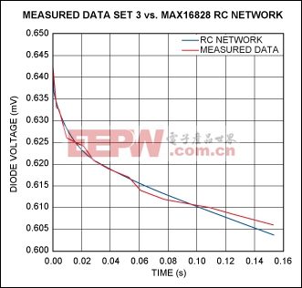
Figure 15. Measured vs. curve-fitted results for the chip's heating curve when the die is dissipating 1.223W.
These experimental results show that the measured results closely match the theoretical model. Such modeling is useful for simulating the transient temperature of an IC, once you have modeled the RC network for that particular chip. The model can also be used for chips of similar size to determine their thermal characteristics during the definition phase. That capability can indicate the operational limitations of the chip. That information, in turn, helps you define the chip's operational modes to prevent overheating.
Conclusion
This article has described a way to model the thermal behavior of a chip as an RC network, which can then be simulated easily using a SPICE tool. The following measures can improve the accuracy of this model:
- Take data at both extremes of power dissipation and at one level in the middle. Fitting the RC network to all three levels simultaneously makes the model usable for most practical power-dissipation levels.
- Improve model accuracy by collecting data points at different ambient temperatures.
These exercises should improve accuracy when necessary, but most applications do not require that you know the temperature with high accuracy. Applications and design engineers, as well as system designers may find the method useful. For more detailed chip information, a company can create RC network models for its ICs and make them available with the chips' corresponding SPICE models.


评论